
Implementation of random logic,Prototyping,Reconfigurable hardware,Hardware dedicated to solving one problem
• DSP
48 can perform mathematical functions such as:
• Add/Subtract
• Accumulate
• Multiply
• Multiply-Accumulate
• Multiplexer
• Barrel
Shifter
• Counter
• Divide
(multi-cycle)
• Square
Root (multi-cycle)
• Can
also create filters such as:
• Serial
FIR Filter (Xilinx calls this MACC filters)
• Parallel
FIR Filter
• Semi-Parallel
FIR Filter
• Multi-rate
FIR Filters
High-performance
FPGA families
Virtex (220 nm)
Virtex-E,
Virtex-EM (180 nm)
Virtex-II (130
nm)
Virtex-II PRO (130 nm)
Virtex-4 (90 nm)
Virtex-5 (65 nm)
Virtex-6
(40 nm)
Virtex-7 (28 nm)
• Low
Cost Family
– Spartan/XL
– derived from XC4000
– Spartan-II
– derived from Virtex
– Spartan-IIE
– derived from Virtex-E
– Spartan-3 (90 nm)
– Spartan-3E (90 nm) –
logic optimized
– Spartan-3A (90 nm) –
I/O optimized
– Spartan-3AN (90 nm) –
non-volatile,
– Spartan-3A DSP (90 nm) –
DSP optimized
– Spartan-6
(45 nm)
– Artix-7
(28 nm)
• Starting
with Virtex 4 family, Xilinx introduced DSP48 block for high-speed DSP on FPGAs
• Essentially
a multiply-accumulate core with many other features
• Now
also in Spartan-3A, Spartan 6, Virtex 5, and Virtex 6
Embedded memories
The M4K memory blocks support the following modes:
v Single-port RAM
(RAM:1-Port)
v Simple dual-port RAM (RAM:
2-Port)
v True dual-port
RAM (RAM:2-Port)
v Tri-port RAM
(RAM:3-Port)
v Single-port ROM
(ROM:1-Port)
v Dual-port ROM
(ROM:2-Port)
Change in Supply Voltages
Year Technology
(nm) Core Supply Voltage (V)
1998 350 3.3
1999 250 2.5
2000 180 1.8
2001 150 1.5
2003 130 1.2
2008 65 1.0
2009 40 0.9
2011
28
0.9
Multiple
Standards for High-Speed Serial Communication
Fibre Channel
InfiniBand
PCI Express (developed by Intel)
RapidIO
SkyRail (developed by MindSpeed Technologies)
10-gigabit Ethernet
Field Programmable Gate Array
Simple’ Programmable Logic Blocks
Massive Fabric of Programmable Interconnects
Standard CMOS Integrated Circuit fabrication process as for
memory chips (Moore’s Law)
An FPGA
contains a set of programmable logic gates and rich interconnect resources,
making it possible to implement complex digital circuits
To simplify the design of
complex systems in FPGAs, there exists libraries of pre-defined complex functions
and circuits (IP cores) that have been tested and optimized to speed up the
design process.
All done by CAD system (e.g.
Xilinx, Quartus)
Chop up circuit into little pieces of logic
Each piece goes in a separate logic element (LE)
Hook them together with the programmable routing
Logic Functions implemented in Look Up Table LUTs.
Flip-Flops. Registers. Clocked
Storage elements.
Multiplexers (select 1 of N inputs)
Huge Density of Logic Block ‘Islands’
1,000 … 100,000’s
in a ‘Sea’ of Interconnects
FPGA Features
Large Complex Functions
Re-Programmability, Flexibility.
Massively Parallel Architecture
Processing many channels simultaneously cf MicroProcessor
Fast Turnaround Designs ,Standard IC Manufacturing Processes.
Moore’s Law
Mass produced. Inexpensive. Many variants. Sizes. Features.
PP Not Radiation Hard L
Power Hungry ,No Analogue
LUT
LUT contains Memory Cells to implement small logic functions
Each cell holds ‘0’ or ‘1’ .
Programmed with outputs of Truth Table
Inputs select content of one of the cells as output
Larger Logic Functions built up by connecting many Logic Blocks
together
Determined by SRAM cells
LUT AS DISTRIBUTED RAM
• CLB LUT configurable as
Distributed RAM
– An LUT equals 16x1 RAM
– Implements Single and
Dual-Ports
– Cascade LUTs to increase RAM size
• Synchronous write
• Synchronous/Asynchronous read
– Accompanying flip-flops used for
synchronous read
• When the CLB LUT is
configured as memory, it can implement 16x1 synchronous RAM. One LUT can
implement 16x1 Single-Port RAM. Two LUTs are used to implement 16x1 dual port
RAM. The LUTs can be cascaded for desired memory depth and width.
• The write operation is
synchronous. The read operation is asynchronous and can be made
synchronous by using the accompanying flip flops of the CLB LUT.
• The distributed ram is
compact and fast which makes it ideal for small ram based functions.
LUT AS SHIFT REGISTER
• Each LUT can be configured as
shift register
– Serial in, serial out
• Dynamically addressable delay
up to 16 cycles
• For programmable pipeline
• Cascade for greater cycle
delays
• Use CLB flip-flops to
add depth
The LUT can be configured as a shift register (serial in, serial
out) with bit width programmable from 1 to 16.
For example, DEPTH[3:0] = 0010(binary) means that the shift
register is 3-bit wide. In the simplest case, a 16 bit shift register can be
implemented in a LUT, eliminating the need for 16 flip flops, and also
eliminating extra routing resources that would have been lowered the
performance otherwise.
FAST CARRY LOGIC
Each CLB contains separate logic and routing for the fast
generation of sum & carry signals
– Increases efficiency and
performance of adders, subtractors, accumulators, comparators, and counters
Carry logic is independent of normal logic and routing resources
All major synthesis tools can infer carry logic for arithmetic
functions
– Addition (SUM = A + B)
– Subtraction (DIFF = A - B)
– Comparators (if A < B then…)
– Counters (count = count +1)
CLB
Each slice contains two sets of the following:
– Four-input LUT
• Any 4-input logic function,
• or 16-bit x 1 sync RAM
(SLICEM only)
• or 16-bit shift register
(SLICEM only)
– Carry & Control
• Fast arithmetic logic
• Multiplier logic
• Multiplexer logic
– Storage element
• Latch or flip-flop
• Set and reset
• True or inverted inputs
• Sync. or async. control
– Each Virtexä-II CLB
contains four slices
– Local routing provides feedback
between slices in the same CLB, and it provides routing to
neighboring CLBs
– A switch matrix provides access to
general routing resources
– Each slice has four outputs
– Two registered
outputs,
two non-registered outputs
– Two BUFTs associated
with each CLB, accessible
by all 16 CLB outputs
– Carry logic runs vertically,
up only
– Two independent
carry chains per CLB
IOB
• IOB provides interface
between the package pins and CLBs
• Each IOB can work as uni- or
bi-directional I/O
• Outputs can be forced into
High Impedance
• Inputs and outputs can be
registered
– advised for high-performance I/O
• Inputs can be delayed
SELECTED IO
• Allows direct connections to
external signals of varied voltages and thresholds
– Optimizes the speed/noise tradeoff
– Saves having to place interface
components onto your board
• Differential signaling
standards
– LVDS (Low Voltage Differential
Signaling), BLVDS, ULVDS
– LDT (Lightning Data Transport)
– LVPECL (Low Voltage Pseudo Emitter
Coupled Logic)
• Single-ended I/O standards
– LVTTL, LVCMOS (3.3V, 2.5V, 1.8V,
and 1.5V)
– PCI-X at 133 MHz, PCI (3.3V at 33
MHz and 66 MHz)
– GTL, GTLP
– and more!
MEMORY AND CLOCKING
• Distributed RAM and Block RAM
– Distributed RAM uses the CLB
resources
– Block RAM is a dedicated resource
on the device (18-kb blocks)
• Dedicated 18 x 18 multipliers
next to block RAMs
• Clock management resources
– 16 dedicated global clock
multiplexers
– Digital Clock Managers (DCMs)
DISTRIBUTED SELECT RAM
• Uses a LUT in a slice as
memory
• Synchronous write
• Asynchronous read
– Accompanying flip-flops
can be used to create
synchronous read
• Emulated dual-port RAM
– One read/write port
One read-only port
BRAM
• The Block RAM is true dual
port, which means it has 2 independent Read and Write ports and these ports can
be read and/or written simultaneously, independent of each other.
• All control logic is
implemented within the RAM so no additional CLB logic is required to implement
dual port configuration.
• Most efficient memory
implementation
• Dedicated blocks of memory
• Ideal for most memory
requirements
• 4 to 104 memory blocks
• 18 kbits = 18,432 bits per
block (16 k without parity bits)
• Use multiple blocks for
larger memories
• Builds both single and true
dual-port RAMs
• Block SelectRAM™ resources
are dedicated resources on the silicon.
• RAMs can be given an initial
value. Many “initialization” attributes are associated with the Block SelectRAM
resources:
• INIT_xx: Numbered attributes
(00 - 3F) that specify the initial memory data contents. Each INIT_xx
attribute is a 64-digit hex number.
• INITP_xx: Numbered attributes
(00 - 07) that specify the initial memory parity contents. Each INITP_xx
attribute is a 64-digit hex number.
• INIT_A/INIT_B: Specifies the
initial value of the RAM output latches after configuration.
• SRVAL_A/SRVAL_B: Specifies
the value of the RAM output latches after SSRA/SSRB is asserted.
• INIT and SRVAL attributes are
specified as hex numbers.
• Up to 3.5 Mb of RAM in 18-kb
blocks
• Synchronous read and write
• True dual-port memory
• Each port has synchronous
read and write capability
• Different clocks for each
port
• Supports initial values
• Synchronous reset on output
latches
• Supports parity bits
• One parity bit per eight data
bits
DUAL PORTS
• Each port can be configured
with a different data bus width
• Provides easy data width
conversion without any additional logic
• Because the RAM blocks
are true dual port, each port can be configured for a different width. This
example shows port A configured as 1K x 4 and port B configured as 256 x16.
This feature can be used for applications requiring different bus widths
for two applications.
• Note that the Altera FLEX 10K
and ACEX 1K families do not have this feature, as they do not have true dual
port capability.
ADDED ADVANTAGE OF TRUE DUAL PORT
• Added advantage of True
Dual-Port
– No wasted RAM Bits
• Can split a Dual-Port 16K RAM
into two Single-Port 8K RAM
Simultaneous independent access
• To access the lower RAM
– Tie the MSB address bit to
Logic Low
• To access the upper RAM
– Tie the MSB address bit to
Logic High
TWO INDEPENDENT SINGLE PORT
• Here, a single 4K bit memory block
is split into two independent 2K bit Single-Port blocks. This feature
allows efficient utilization of memory bits. The upper 2K bit block is accessed
by tying the ADDR11 bit to Vcc whereas the lower 2K bit block is accessed by
tying it to GND instead.
DEDICATED MULTIPLER BLOCKS
• 18-bit two’s complement
signed operation
• Optimized to implement
Multiply and Accumulate functions
• Multipliers are physically
located next to Block SelectRAM™ memory
GLOBAL CLOCK ROUTING RESOURCES
• Sixteen dedicated global
clock multiplexers
• Eight on the top-center of
the die, eight on the bottom-center
• Driven by a clock input pad,
a DCM, or local routing
• Global clock multiplexers
provide the following:
• Traditional clock buffer
(BUFG) function
• Global clock enable
capability (BUFGCE)
• Glitch-free switching between
clock signals (BUFGMUX)
• Up to eight clock nets can be
used in each clock region of the device
Each device contains four or more clock regions
DCM
• Up to twelve DCMs per device
– Located on the top and bottom edges
of the die
– Driven by clock input pads
• DCMs provide the following:
– Delay-Locked Loop (DLL)
– Digital Frequency Synthesizer (DFS)
– Digital Phase Shifter (DPS)
• Up to four outputs of each
DCM can drive onto global clock buffers
All DCM outputs can drive general routing
CLOCKED LOGIC:
Registers on outputs. CLOCKED storage elements.
Synchronous FPGA Logic Design, Pipelined Logic.
FPGA Fabric Pulse from Global Clock (e.g. LHC BX frequency)
FPGA Classification
Based on Functional Unit/Logic Cell Structure
v Transistor Pairs
v Basic Logic Gates: NAND/NOR
v MUX
v Look –up Tables (LUT)
v Wide-Fan-In AND-OR Gates
Programming Technology
v Anti-Fuse Technology
v SRAM Technology
v EPROM Technology
• Vary from vendor to vendor.
All share the common property: Configurable in one of the two positions – ‘ON’
or ‘OFF’
• Can be classified into three
categories:
– SRAM based
– Fuse based
– EPROM/EEPROM/Flash based
• Desired properties:
• Minimum area consumption
• Low ON resistance; High OFF
resistance
• Low parasitic capacitance to
the attached wire
• Reliability in volume
production
– SRAM cells are used
• As Look-Up Tables (LUT) to
implement logic (as Truth Tables)
• As embedded RAM blocks (for
buffer storage etc.)
• As control to routing and
configuration switches
– Advantages
• Allows In-System Programming
(ISP)
• Suitable for Reconfigurable
HW
– Disadvantages
• Volatile – needs power all
the time / use PROM to
download configuration data
ANTIFUSE
v Invented at Stanford and developed by Actel
v Opposite to regular fuse Technology - Normally an
open circuit until a programming current (about 5 mA) is forced through
it
v Two Types:
1) Actel’s PLICE [Programmable
Low-Impedance Circuit Element] - A High-Resistance Poly-Diffusion
Antifuse
2) QuickLogic’s Low-Resistance
metal-metal antifuse [ViaLink] technology
ü Direct metal-2-metal connections
ü Higher programming currents reduce antifuse
resistance
v Disadvantages:
1) Unwanted Long Delay
EPROM
• EPROM Programming Technology
– Two gates: Floating and Select
– Normal mode:
• No charge on floating gate
• Transistor behaves as normal
n-channel transistor
– Floating gate charged by applying
high voltage
• Threshold of transistor (as
seen by gate) increases
• Transistor turned off
permanently
– Re-programmable by exposing to UV
radiation
• Not in-system re-programmable
• Re-programming is a time
consuming task
• Two gates: Floating and
Select
• Functionally equivalent to
EPROM; Construction and structure differ
• Electrically Erasable:
Re-programmable by applying high voltage
(No UV radiation exposure!)
• When un-programmed, the
threshold (as seen by select gate) is negative!
• Re-programmable; In general,
in-system re-programmable
• Re-programming consumes
lesser time compared to EPROM technology
• Multiple voltage sources may
be required
• Area occupied is twice
that of EPROM!
All FPGAs contain the same basic resources
– Slices (grouped into CLBs)
• Contain combinatorial logic
and register resources
– IOBs
• Interface between the FPGA
and the outside world
– Programmable interconnect
– Other resources
• Memory
• Multipliers
• Global clock buffers
• Boundary scan logic
Configuring of FPGA
Millions of SRAM cells holding LUTs and Interconnect Routing
Volatile Memory. Lose configuration when board power is turned
off.
Keep Bit Pattern describing the SRAM cells in non-Volatile Memory
e.g. PROM
Configuration takes ~ secs
FPGA Trends
State of Art is 40nm on 300 mm wafers
Top of range >500,000 Logic Blocks
>1,000 pins (Fine Pitched BGA)
Logic Block cost ~ 1$ in 1990
Today < 0.1 cent
Problems
Power. Leakage currents.
Design Gap
CAE Tool
FPGA design where a reset acts as a synchronization signal that sets all the storage elements to a known state. In a digital design, designers normally implement a global reset as an external pin to initialize the design on power-up. The global reset pin is similar to any other input pin and is often applied asynchronously to the FPGA.
Designers can then choose to use this signal to reset their design asynchronously or synchronously inside the FPGA. An optimal reset structure will enhance device utilization, timing and power consumption in an FPGA.
Devices in the Xilinx 7 series architecture contain eight registers per slice, and all these registers are D-type flip-flops. All of these flip-flops share a common control set.The control set of a flip-flop is the clock input (CLK), the active-high chip enable (CE) and the active-high SR port. The SR port in a flip-flop can serve as a synchronous set/reset or an asynchronous preset/clear port.
The RTL code that infers the flip-flop also infers the type of reset a flip-flop will use. The code will infer an asynchronous reset when the reset signal is present in the sensitivity list of an RTL process . The synthesis tool will infer a flip-flop with an SR port configured as a preset or clear port . When the SR port is asserted, the flip-flop output is immediately forced to the SRVAL attribute of the flip-flop. In the case of synchronous resets, the synthesis tool will infer a flip-flop whose SR port is configured as a set or reset port.In addition, you can initialize the flip-flop output to the value the INIT attribute specifies. The INIT value is loaded into the flip-flop during configuration and when the global set reset (GSR) signal is asserted.
The flip-flops in Xilinx FPGAs can support both asynchronous and synchronous reset and set controls. However, the underlying flip-flop can natively implement only one set / reset / preset / clear at a time. Coding for more than one set / reset / preset / clear condition in the RTL code will result in the implementation of one condition using the SR port of the flip-flop and the other conditions in fabric logic, thus using more FPGA resources.
If one of the conditions is synchronous and the other is asynchronous, the asynchronous condition will be implemented using the SR port and the synchronous condition in fabric logic. In general, it’s best to avoid more than one set/reset/preset/clear condition. Furthermore, only one attribute for each group of four flip-flops in a slice determines if the SR ports of flip-flops are synchronous or asynchronous.
Regardless of the reset type used (synchronous or asynchronous), you will generally need to synchronize the reset with the clock. As long as the duration of the global reset pulse is long enough, all the device flip-flops will enter the reset state. However, the deassertion of the reset signal must satisfy the timing requirements of the flip-flops to ensure that the flip-flops transition cleanly from their reset state to their normal state. Failure to meet this requirement can result in flip-flops entering a metastable state. Furthermore, for correct operation of some subsystems, like state machines and counters, all flip-flops must come out of reset on the same clock edge. If different bits of the same state machine come out of reset on different clocks, the state machine may transition into an illegal state. This reinforces the need to make the deassertion of reset synchronous to the clock.
For designs that use a synchronous reset methodology for a given clock domain, it is sufficient to use a standard metastability resolution circuit (two back-to-back flip-flops) to synchronize the global reset pin onto a particular clock domain. This synchronized reset signal can then initialize all storage elements in the clock domain by using the synchronous SR port on the flip-flops. Because both the synchronizer and the flip-flops to be reset are on the same clock domain, the standard PERIOD constraint of the clock covers the timing of the paths between them. Each clock domain in the device needs to use a separate synchronizer to generate a synchronized version of the global reset for that clock domain.
Sometimes a portion of a design is not guaranteed to have a valid clock. This can occur in systems that use recovered clocks or clocks that are sourced by a hot-pluggable module. In such cases, the storage elements in the design may need to be initialized with an asynchronous reset using the asynchronous SR port on the flip-flops. Even though the storage elements use an asynchronous SR port, the deasserting edge of the reset must still be synchronous to the clock. This requirement is characterized by the reset-recovery timing arc of the flip-flops, which is similar to a setup requirement of the deasserting edge of an asynchronous SR to the rising edge of the clock. Failure to meet this timing arc can cause flip-flops to enter a metastable state and synchronous subsystems to enter unwanted states.
You can see the change
in slack
Description:
Generate a new clock object from an existing
physical clock object in the
design.
Clocks can be added to a design in one of
three ways:
*
Primary physical or virtual clocks defined with the create_clock command.
*
Derived clocks defined with the create_generated_clock command
generated from a primary physical clock.
*
Derived clocks automatically generated by the Vivado Design Suite when
a clock propagates to an MMCM/PLL/BUFR.
You can also use the create_generated_clock
command to change the name of clocks
that the Vivado tool has auto-derived from an MMCM/PLL/BUFR. In this case, a new clock is not created, but an
existing clock defined on the specified
source object is renamed to the provided name. This requires -name and <object> to be specified, and
supports the use of -source and/or -master_clock to further identify the clock
to rename when multiple clocks exist on
the source object. Refer to the Vivado Design Suite User Guide:
Using Constraints (UG903) for more
information on renaming auto-derived clocks.
Note: You cannot rename a clock that is
already in use by other constraints at
the time of renaming. You must rename the clock prior to any other appearance or use of the clock in an XDC file
This command returns the name of the clock
object that is created, or returns an
error if it fails.
Arguments:
-name <arg> - (Optional) The name of
the generated clock to create on the specified object, or the name to assign to an
existing clock on the specified object.
If no name is specified, the generated clock will be given the name of the <object> it is
assigned to. If assigned to multiple
<objects>, the name will be the first
object in the list.
-source <arg> - (Optional) The pin or
port of the master clock from which to
derive the generated clock. The master clock must be a previously defined physical clock, not a virtual clock;
but can be a primary clock or another
generated clock. If the source pin or port currently has multiple clocks defined, the -master_clock option must
be used to identify which clock on the
source is to be used to define the generated clock.
-edges< <arg> - (Optional) Specifies
the edges of the master clock to use in
defining transitions on the generated clock. Specify transitions on the generated clock in a sequence of 1, 2, 3, by
referencing the appropriate edge count
from the master clock in numerical order, counting from the first edge. The sequence of transitions on
the generated clock defines the period
and duty cycle of the clock: position 1 is the first rising edge of the generated clock, position 2 is the first
falling edge of the generated clock and
so defines the duty cycle, position 3 is the second rising edge of the generated clock and so defines the
clock period. Enclose multiple edge
numbers in braces {}. See the example below for specifying edge numbers.
-divide_by <arg> - (Optional) Divide the
frequency of the master clock by the
specified value to establish the frequency of the generated clock object. The value specified must be >= 1,
and must be specified as an integer.
-multiply_by <arg> - (Optional)
Multiply the frequency of the master clock by the specified value to establish the
frequency of the generated clock object. The value specified must be >= 1,
and must be specified as an integer.
-combinational - (Optional) Define a
combinational path to create a "-divide_by 1" generated clock.
-duty_cycle< <arg> - (Optional) The
duty cycle of the generated clock defined as a percentage of the new clock
period when used with the -multiply_by
argument. The value is specified as a percentage from 0.0 to 100.
-invert - (Optional) Create a generated clock
with the phase inverted from the master
clock.
-edge_shift <arg> - (Optional) Shift
the edges of the generated clock by the
specified values relative to the master clock. See the example below for specifying edge shift.
-add - (Optional) Add the generated clock
object to an existing clock group specified by <objects>.
Note: -master_clock and -name options must be
specified with –add -master_clock
<arg> - (Optional) If there are multiple clocks found on the source pin or port, the specified clock
object is the one to use as the master
for the generated clock object.
Note: -add and -name options must be
specified with -master_clock -quiet -
(Optional) Execute the command quietly, returning no messages from the command. The command also returns TCL_OK
regardless of any errors encountered
during execution.
Note: Any errors encountered on the
command-line, while launching the command, will be returned. Only errors
occurring inside the command will be trapped.
-verbose - (Optional) Temporarily override
any message limits and return all
messages from this command.
Note: Message limits can be defined with the
set_msg_config command.
<objects> - (Required) The pin or port
objects to which the generated clock should be assigned. If the specified objects
already have a clock defined, use the
-add option to add the new generated clock and not overwrite any existing clocks on the object.
Examples:
The following example defines a generated
clock that is divided from the master
clock found on the specified CLK pin. Since -name is not specified, the generated clock is assigned the same name
as the pin it is assigned to:
create_generated_clock -divide_by 2 -source
[get_pins clkgen/sysClk] fftEngine/clk
The following example defines a generated
clock named CLK1 from the specified
source clock, specifying the edges of the master clock to use as transition points for the generated clock, with
edges shifted by the specified amount.
In this example, the -edges option indicates that the second edge of the source clock is the first
rising edge of the generated clock, the
third edge of the source clock is the first falling edge of the generated clock, and the eighth edge of the
source clock is the second rising edge
of the generated clock. These values determine the period of the generated clock as the time from edge 2
to edge 8 of the source clock,
and the duty cycle as the percentage of the
period between edge 2 and edge
3 of the source clock. In addition, each edge
of the generated clock is
shifted by the specified amount:
create_generated_clock -name CLK1 -source
CMB/CLKIN -edges {2 3 8} \
-edge_shift {0 -1.0 -2.0} CMB/CLKOUT
Note: The waveform pattern of the generated
clock is repeated based on the
transitions defined by the -edges argument.
This example creates two generated clocks
from the output of a MUX, using
-master_clock to identify which clock to use,
using -add to assign the
generated clocks to the Q pin of a flip flop,
and using -name to define a
name for the generated clock, since the
object it is assigned to has
multiple clocks assigned:
create_generated_clock -source [get_pins
muxOut] -master_clock M_CLKA \
-divide_by 2 -add -name gen_CLKA [get_pins
flop_Q]
create_generated_clock -source [get_pins
muxOut] -master_clock M_CLKB \
-divide_by 2 -add -name gen_CLKB [get_pins
flop_Q]
The following example renames the
automatically named clock that is derived
by the Vivado Design Suite on the MMCM clock
output:
create_generated_clock -name CLK_DIV2
[get_pins mmcm/CLKOUT1]
See Also:
*
check_timing
*
create_clock
*
get_generated_clocks
* get_pins
*
report_clock
*
set_clock_latency
*
set_clock_uncertainty
*
set_propagated_clock
Generated clocks are driven inside
the design by special cells called Clock Modifying Blocks (for example, an
MMCM), or by some user logic.
The XDC command
"create_generated_clock" is used to create a generated clock object.
Syntax:
create_generated_clock [-name
<arg>] [-source <args>] [-edges <args>]
[-divide_by <arg>]
[-multiply_by <arg>]
[-combinational] [-duty_cycle
<arg>] [-invert]
[-edge_shift <args>]
[-add] [-master_clock <arg>]
[-quiet] [-verbose]
<objects>
This article discusses the common
use cases of creating a generated clock.
For more information on
create_generated_clock, please refer to (UG903).
Solution
Generated clocks are associated with
a master clock from which they are derived.
The master clock can be a primary
clock or another generated clock.
Please ensure you define all primary
clocks first.
They are required for defining the
generated clocks.
Use Case 1: Automatically Derived
Clocks
For Clock Modifying Blocks (CMB)
such as MMCMx, PLLx,IBUFDS_GTE2, BUFR and PHASER_x primitives, you do not need
to manually create the generated clocks.
Vivado automatically creates these
clocks, provided the associated master clock has already been defined.
You only need to create the primary
clock that is feeding into the CMB.
The auto-generated clock names can
be reported by the report_clocks command in the synthesized or implemented
design so that you can use them in other commands or constraints.
It is possible to force the name of
the generated clock that is automatically created by the tool.
See "Use Case 2: Renaming
Auto-derived Clocks" below.
An auto-generated clock is not
created if a user-defined clock (primary or generated) is also defined on the
same netlist object, that is, on the same definition point (net or pin).
Vivado gives the following warning
message when an existing primary or generated clock prevents auto-generated
clock propagation:
Warning:[Timing 38-3] User defined
clock exists on pin <pin_name> and will prevent any subsequent automatic
derivation.
Automatically Derived Clock Example
The following automatically derived
clock example is a clock generated by an MMCM.

XDC constraint:
create_clock -name clkin -period 10.000 [get_ports clkin]
The report_clocks command prints the
following information:
Clock Period Waveform Attributes
Sources
clkin 10.00000 {0.00000 5.00000} P
{clkin}
cpuClk 10.00000 {0.00000 5.00000}
P,G {clkip/mmcm0/CLKOUT}
Use Case 2: Renaming Auto-derived
Clocks
It is possible to force the name of
the generated clock that is automatically created by the tool.
The renaming process consists of
calling the create_generated_clock command with a limited number of parameters.
create_generated_clock -name new_name [-source source_pin]
[-master_clock master_clk] source_object
A single create_generated_clock
command has to specify a unique auto-derived clock to rename.
A user-defined generated clock
cannot be renamed.
Renaming Auto-derived Clock Example
Same example in Use Case 1:
XDC constraint:
create_clock -name clkin -period
10.000 [get_ports clkin]
#renaming auto-derived clock cpuClk
create_generated_clock -name user_clk [get_pins clkip/mmcm0/CLKOUT]
Then the report_clocks command
prints the following information:
Clock Period Waveform Attributes
Sources
clkin 10.00000 {0.00000 5.00000} P
{clkin}
user_clk 10.00000 {0.00000 5.00000}
P,G {clkip/mmcm0/CLKOUT}
......
Use Case 3: User Defined Generated
Clocks
When no automatic generation occurs,
you will need to manually create clock modifications.
For example, for a clock divider
logic that consists of LUTs and FFs, Vivado is not aware of the period
relationship between the source clock and the divided clock.
As a result, a user-defined
generated clock is required for the divided clock.
This type of clock divider is not
recommended in an FGPA. We recommend using an MMCM or a PLL to divide the
clock.
Specify the master source using the
-source option.
This indicates a pin or port in the design through which the master clock
propagates.
It is common to use the master clock source point or the input clock pin of a
generated clock source cell.
User Defined Generated Clock Example
The primary clock drives a register
divider to create a divide-by-2 clock at the register output.

Two equivalent constraints are
provided below:
create_clock -name clkin -period 10 [get_ports clkin]
# Option 1: master clock source is the primary clock source point
with a 'divide by' value of the circuit.
create_generated_clock -name clkdiv2 -source [get_ports clkin]
-divide_by 2 [get_pins REGA/Q]
# Option 2: master clock source is the REGA clock pin with a
'divide by' value of the circuit.
create_generated_clock -name clkdiv2 -source [get_pins REGA/C]
-divide_by 2 [get_pins REGA/Q]
Use Case 4: Forwarded Clock through
ODDR
In the Source Synchronous
application, the clock is regenerated in the source device and forwarded to the
destination device along with data.
A common method is to use clock
forwarding via a double data-rate register.
In the following example, the ODDR
instance in the source device is used to generate the forwarding clock for the
Source Synchronous interface.
A user-defined generated clock needs
to be created for the forwarding clock in order to be used in the
set_output_delay constraint for the Source Synchronous interface.
Example of Creating Generated Clock at Clock Output Port:

create_generated_clock -name fwd_clk -multiply_by 1 -source
[get_pins ODDR_inst/C] [get_ports CLKOUT]
The generated clock can then be referenced in the set_output_delay command.
For more information on set_output_delay
command, please refer to (UG903).
Use Case 5: Overlapping Clocks
Driven by a Clock Multiplexer
When two or more clocks drive into a
multiplexer (or more generally a combinatorial cell), they all propagate
through and become overlapped on the fanout of the cell.
For this reason, you must review the
CDC paths and add new constraints to exclude false paths due to overlapping.
The correct constraints are dictated
by how and where the clocks interact in the design.
In some scenarios, user-defined
generated clocks need to be created for the multiplexed clock in order to
correctly constrain the CDC paths.
Multiplexed Clock Example:

If clk0 and clk1 only interact in
the fanout of the multiplexer (FDM0 and FDM1), (i.e. the paths A, B and C do not
exist), it is safe to apply the clock groups constraint to clk0 and clk1
directly.
set_clock_groups -logically_exclusive -group clk0 -group clk1
If clk0 and/or clk1 directly interact with the multiplexed clock (i.e. the
paths A or B or C exist), then in order to keep timing for paths A, B and C,
the constraint cannot be applied to clk0 and clk1 directly.
Instead, it must be applied to the
portion of the clocks in the fanout of the multiplexer, which requires
additional clock definitions.
In this case, two generated clocks
are created at the Multiplexer output pin and paths crossing the generated
clock domains are ignored.
create_generated_clock -name clk0mux -divide_by 1 -source
[get_pins mux/I0] [get_pins mux/O]
create_generated_clock -name clk1mux -divide_by 1 -add
-master_clock clk1 -source [get_pins mux/I1] [get_pins mux/O]
set_clock_groups -physically_exclusive -group clk0mux -group
clk1mux
have
a design consisting of Clock Wizard IP(MMCM) with input clock 100MHz at
"clk_in1". Now I generate 50MHz clock at output "clk_out1".
As per UG903(Page 88 and 89), Xilinx automatically derives constraints
"create_generated_clock" for the clocks generated using PLL, MMCM
etc.
But when I checked my design I cannot see any
"create_generated_clock" constraints defined automatically for the
"clk_out1".
You only
need to create_clock for the input port of MMCM, then the output clock of MMCM
will be automatically generated. You don't need to create_generated_clock on
the output of MMCM manually.
You can
check the result of report_clocks to see the auto-generated clocks.
Ex: clk_pin_p
is the input clock for MMCM, clk_rx_clk_core/clk_tx_clk_core is the output
of MMCM.
The following example
shows the use of the multiple through points to
define both a specific path (through
state_reg1) and alternate paths
(through count_3 or count_4), and writes the
timing results to the
specified file:
report_timing -from go -through
{state_reg1} -through { count_3 count_4
} \
-to done -path_type summary -file
C:/Data/timing1.txt
report_timing
–from[get_pins clk_in_IBUF_BUFG_inst/ clk_in_IBUF_inst] –to[get_pins
freq_cnt_reg[24]/R]
During the micro-architecture or detailed design phase FPGA resource requirements shall be estimated. Module designers shall have “detailed view” of the design down to function/majorcomponent level for near-accurate estimates. At the end of this phase, exact FPGA part to be used shall be finalized from the chosen family.
Following are critical aspects that need to be considered during this phase:
1. FPGA device Architecture: Detailed investigation and understanding of FPGA device architecture/capabilities including logic cells, RAMs, multipliers, DLL/PLL and IOs
2. Module boundaries: All modules interfaces shall be on register boundary.
3. Internal bus structure: A well defined internal point-to-point bus structure is preferred than routing all signals back and forth.
4. Clocks: Clock multiplexing and gating shall be avoided and if required shall be done based on device capabilities
5. Resets: Number of resets in the system shall be optimized based on dedicated reset routingresources available
6. Register file: Instead of creating one common register file and routing register values to all modules; it is better to have registers wherever they are used. If needed even registers may be duplicated. It should be noted that though write path may be of multi-cycle path, but read path may not be. Also registers shall be implemented in RAM wherever possible
7. Selection of memories/multipliers: The memory size requirement shall decide whether to use hard-macros or to build with logic. For small size memories, it is not at all preferred to map to large memory hard-macros, though it might take additional logic resources. The primary reason for this is hard-macro memory locations are fixed and placing driving/receiving logic next to memories is not always possible. Similarly, it is not advantageous to map small multiplier (such as 3x3) to an 18x18 hard- macro multiplier.
8. Data/Control path mixing: Often it is advantageous to store control signals along with data bits in memories and pass-on to other modules. For example let us consider 16 data bits and 2 control bits to be transferred from one module to another through memory. These 18 bits can be stored as data bits in available block-memory of size say 1kx18 block memories. Also this method will be further advantageous if the hand-shake is asynchronous.
9. Big multiplexer structures: It is not preferred to build very big multiplexer structures (say 256:1) especially for timing critical paths. Instead smaller multiplexers can be built, which are more controllable.
10. High-level Floorplan: A high-level floorplan including IO planning shall be worked-out (as shown in Figure 1) based on the gate count and other macro estimates. Also spare area shall be planned for future/field upgrades. At this stage it is not necessary to fix the IO locations but it is necessary to fix the IO banks in FPGA. Having done the high level floorplan; the budgeted area shall be known to module level designers. Also interface module floorplan locations shall be known to the module level designers, which will enable them to further floorplan allocated area if necessary. Some of the high level floorplanning considerations are:
a. Controlling congestion along with proximity
b. Draw the data flow diagram of the design with the memories that are used to terminate the data paths and do module level area allocation
c. Interdependent modules should be closer
d. Module level area allocated shall be close to Macros which it is interfacing to
e. Free area (rows and columns) between module area allocations, which will aid in inter module routing in full chip
f. Clock resources and routing limitations if any
11. Module output replication: Based on the initial floorplan each module output might have to be replicated if modules receiving this data are located in different corners of the chip.
12. Best practices: RTL coding guidelines shall be passed on to module level designers.
RTL coding phase
Following are critical aspects which need to be considered during RTL coding phase:
1. Logic delay: Though it may be adequate to maintain logic delay of around 50%, it is desirable to maintain high speed paths in the design lower than that, say to 20-30%. Usually there are abundant resources such as Flip Flops (normally 1 flip flop for each look-up table), RAMs, and Multipliers etc. Wherever it doesn’t affect throughput, additional pipeline stages can be introduced judiciously keeping in mind the routing congestion issues.
2. Device mapping efficiency: The RTL code shall enable best FPGA mapping by exploring the device architecture. One such example is in Xilinx Virtex2 FPGA there is an additional 2:1 MUX (F5) between 2 LUTs with dedicated routes. If a 4:1 MUX is coded as single entity, it will map well in one slice with 2 LUTs and an F5 MUX. Instead if 4:1 MUX built with pipelining after 2:1 MUX, then it can’t be mapped to F5 MUX and additional slice is needed. Another example is long register based shift register can be mapped to SRL configuration of LUT, provided all these registers need not have reset.
3. Fan-out: Though synthesis tools can do automatic fan-out control, manual control is needed especially for the signals interfacing to hard-macros, as tools will treat every thing in same manner and often they are black-boxes.
4. Vendor specific structures and instantiations: Create hierarchy around them to give freedom to migrate from one technology to another.
5. Macro interface: All the inputs/outputs of macros shall be registered due to their fixed locations.
6. Gated clocks: Avoid gated clocks and use clock enables instead.
7. Critical logic: Place critical logic in separate hierarchy
8. Critical paths: Make sure that they are not crossing hierarchy of the block by registering all the outputs.
9. Tri-state buffers: For low speed paths, it is desirable to use tri-state buffers to save logic cells
10. Unused hard-macros: Unused RAMs can be used as register set or to map state machines coded as look up tables. This will also avoid large multiplexers in the read path. Also unused multipliers can be used as long shifters.
11. False and multi-cycle paths: False and multicycle paths shall not be pipelined and shall be identified by design and pass on to synthesis tool.
12. Trail synthesis and P&R: Each module level designer shall perform individual module level synthesis and P&R of the design with the given floorplan and optimize the RTL code while being developed. If the IO requirement of a module exceeds the device physical IOs, dummy logic can be added to demultiplex/miltiplex few-pins-to-more-pins and/or more-pins-to-few-pins using shift register structures and/or OR-gate structure as shown in Figure 2. Also as shown in this figure insert additional flip-flops on interfaces to selected module to other modules by leaving actual IO interfaces same. This will eliminate skewed timing results due to dummy logic and connections. Also black-box timing information shall be used during synthesis to avoid skewed timing results.
13. Module level Floorplanning: With-in the given floorplan area, often it is desirable to do sub-module level floorplanning. In this submodule level floorplanning it is often necessary to do floorplan only for critical parts of the design. Also it is necessary to do individual synthesis compile of timing critical sub-modules being floorplanned which will prevent hierarchy loss (as shown in Figure 3), and there-by ineffcient placement.
14. Logic compression: Though from area standpoint it is preferred to do maximum level packing of unrelated logic (for example using COMPRESSION with Xilinx flow), it will have adverse impact on timing. Thus unrelated logic packing level shall be set based on timing criticality of each sub-module.
15. IO allocation: The respective module IO fixing shall be done based on IO ring pin sequence on the die rather than pin sequence on the package.
Chip level Synthesis phase
During the chip level synthesis phase, following information shall be collected from individual module designers:
1. Area constraints with unrelated logic compression information
2. Timing constrains including false and multicycle paths
3. IO assignments
4. Black-box timing information
5. Synthesis compile hierarchy
6. Timing critical sub-module information
Module level synthesis has to be carried out with the information gathered from designers. Mere meeting frequency at synthesis stage is not good enough as route estimates are inaccurate. Instead if logic delay achieved is 50% of the cycle time, we can say we have achieved possible best results out of synthesis and move on to further steps.
The resource sharing and fan-out control options in synthesis tool can be enabled for non timing critical sub-modules. Whereas synthesis tool options such as register replication, fan-out control and retiming can be enabled for timing critical submodules. Thus in the chip top level synthesis compilation, all modules will be black-boxes. Automated push-button based physical synthesis has yielded only 10-15% overall improvement in performance after P&R. However there are physical synthesis tools (e.g. Synplify premier) which supports floorplanning at synthesis stage. However the methodology described in this paper is equally applicable to netlist based floorplanning or physical synthesis based design floorplanning.
Timing Analysis
TIMING ANALYSIS
Timing Assertions Section
Primary clocks
Virtual clocks
Generated clocks
Clock Groups
Input and output delay constraints
Timing Exceptions Section
False Paths
Max Delay / Min Delay
Multicycle Paths
Case Analysis
Disable Timing
Physical Constraints Section located anywhere in the file, preferably before or after the timing constraints or stored in a separate constraint file.
Start with the clock definitions.
The clocks must be created before they can be used by any subsequent constraints.
Any reference to a clock before it has been declared results in an error and the corresponding constraint is ignored. This is true within an individual constraint file, as well as across all the XDC files (or Tcl scripts) in your design.
The order of the constraint files matters. You must be sure that the constraints in each file do not rely on the constraints of another file.
If this is the case, you must read the file that contains the constraint dependencies last.
If two constraint files have interdependencies, you must either:
• Merge them manually into one file that contains the proper sequence, or
• Divide the files into several separate files, and order them correctly.
Start with no timing
constraints
Use IDE to view the
clock networks
Create basic clocks
Review Timing reports
for coverage
Open synthesized design
.See schematic
Report clock networks.Click
constraints
See unconstrained
Before editing go for
report_clocks
Edit
timing constraints

Click generated clock
Description:
Create a generated
clock object
Syntax:
create_generated_clock [-name <arg>] [-source <args>]
[-edges <args>]
[-divide_by
<arg>] [-multiply_by <arg>]
[-combinational]
[-duty_cycle <arg>] [-invert]
[-edge_shift
<args>] [-add] [-master_clock <arg>]
[-quiet] [-verbose]
<objects>
Returns:
new clock object
Usage:
Name Description
-----------------------------
[-name] Generated clock name
[-source] Master clock source object pin/port
[-edges] Edge Specification
[-divide_by] Period division factor: Value >= 1
Default: 1
[-multiply_by] Period multiplication factor: Value >= 1
Default: 1
[-combinational] Create a divide_by 1 clock through
combinational logic
[-duty_cycle] Duty cycle for period multiplication:
Range: 0.0 to 100.0
Default: 0.0
[-invert] Invert the signal
[-edge_shift] Edge shift specification
[-add] Add to the existing clock in
source_objects
[-master_clock] Use this clock if multiple clocks present at
master pin
[-quiet] Ignore command errors
[-verbose] Suspend message limits during command
execution
<objects> List of clock source ports, pins, or
nets
Categories:
SDC, XDC
report_timing
if its ports go generic
if it is pins,do tcl
for get_pins
and do
report_timing -from[get_pins ..]-to[get_pins ..]]
view contents of the
report
Timing reports always
start from primary clock propagate to the generated clocks and then on to the
clock elements.
observe the destination path clock timing.
See the requirements of
the generated clock
See the
destination clock start of next clock
edge and on to destination register
Slack is the required
time – arrival time
Open the schematic of
the netlist ,select clk_gen.window.zoom it
Observe the difference
in schematic which is periodically enabled to generate the destination clocks.
In this case,generated
clocks doesnot have the predefined relationship with the primary clocks clk pin
As a result,create a
tcl command
create_generated clock
save the constraints
enter the tcl command
report_clocks
observe the new
generated clock included in the timing reports
click report timing
summary
select new generated
clk
see intraclk path,see
the setup.double click any path to view the path properties
see the source clock
path
source clock delay
starts primary clock and propgate to generated clocks both automatically and
manual generated clocks
see the destination
clock path
starts from primary
clock and propagated to generated clocks
close the properties.
set
input_delay
report_timing
–from[all_inputs]
see the reports
set_input_delay –clock[get_clocks
–phyclk0] –max3$my_input
report_timing
–from$my_input –setup
see the reports
see the slack and input
delay
insert the below tcl
set_input_delay
–clock[get_clocks –phyclk0] –min1$my_input
report_timing
–from$my_input –hold
report shows actual
slack and the input delay
In addition see the
edit timing constraint, can add set_input_delay
set
output_delay
report_timing
–to[all_inputs]
see the reports
set_input_delay
–clock[get clocks –sysclk0] $my_output
report_timing
–from$my_input –hold
see the reports
see the actual slack
and input delay
In addition see the
edit timing constraint, can add set_output_delay
set
clock groups
Open the synthesized
design
Report clock
interaction
Analyze the timing path
from one clock domain to another clock domain
Report shows grid of
clock interactions
Each grid is colored to
indicate timing ,constraint status in inter clock path
If the two clock groups
does not meet timing it is asynchronous
Clock frequencies are
not integer multiples .Its impossible to find the relative fields between them.
report_clock_interactions
–delay_type min_max –significant_digits 3 –name timing_1
see the wns and choose
max
suppose if you have two
constraints like clk_out1_clk_core, clk_out2_clk_core=>
join [get_timing_paths
–from [get_clocks clk_out1_clk_core] –to[get_clocks clk_out2_clk_core]
-max_paths 200]
join [get_timing_paths
–from [get_clocks clk_out2_clk_core] –to[get_clocks clk_out1_clk_core]
-max_paths 200]
Two
clocks marked as asynchronous
Launch
timing contraints-edit
Double
click set clock_group
You
need to specify two clock groups
Add
the first clock group
Add
the second by click + sign
Note
asynchronous is chosen by default.
Save
the constarints
Report
clock interactions
Observe
the interclock path between clock grp1 and 2 is decalred blue confirming
asynchronous
Set false path

report
timing_summary
See
the interclock path
See
the setup
set_false_path
–from[get_pins ]-to[get_pins ]]
report_timing
–from [get_pins ]-to[get_pins ]]
if sklack
is infinite false path is sucessful
if not
check the false path
set multicycle path
report_timing
See
the interclock path
See
the setup

See the vioLated slack
if any
See the requirement

What are the guidelines followed for
good floorplan?
Steps followed with the aim of generating
an optimum floor plan.
1.
Defining the core area using Specify
Floor Plan Form
2.
Defining ports specified by top
level engineer.
3.
Placing the macros inside the core
area.
4.
Placing the Macros which are
communicating with each other, together with help of Fly Lines,
5.
Color by Hierarchy and Data Flow
Diagrams.
6.
Avoid the placement of Macros in
front of ports.
7.
Arrange the Macros to get contiguous
core area.
8.
Defining halos
9.
Defining Placement and Routing
blockages.
3.5 Place & Route phase
During
the chip level P&R phase, following information shall be collected from
synthesis stage along with the netlists:
1.
Area constraints with
unrelated logic compression information
2.
Timing constrains
including false and multicycle paths
3.
IO assignments
4.
Timing critical
sub-module information
As a first step in P&R process, fix the locations of top level primitives such as global clock buffers, DLL/PLL and IOs. After first pass P&R, usually on a complex design the route delays are high and there are many violator paths even after doing module level floorplanning.
At this stage it is better to look for area regions where the route delays are higher rather than trying to solve timing issues one at a time.
Top one or two timing violator areas shall be found and unrelated logic compression shall be reduced and/or area of such region shall be increased. The area left out during high-level floorplan will be helpful here. This process shall be continued till number of timing violators come down to few in number.
At this stage it might be better to go for option of constructing relatively-placed-macros (RPM) for hard to meet timing paths, such as huge multiplexer, FIFO etc.
The core generator tools (such as Coregen from Xilinx) can generate components with RPM. It is also possible to generate custom RPM structures based on floorplan by instantiating FPGA primitives. These macros will be placed as a group of elements in the defined area region.
Especially this RPM structure method is extremely useful for short timing critical paths. After performing all these steps, there may be still last few timing violators.
One way of handling these violators is to open
the place & routed design in FPGA editing tools, and fix by moving elements
around. This is often a tedious manual process, which might even impact other
paths. It would be of great help if P&R tools can automate this process
even under manual guidance by doing what-if analysis.
Distribution – generation (frequency synthesis)
Deskew
Multiplexing
Runtime programming
Domain crossing
Clock Distribution
Device split into halves (top/bottom) and clock regions (rectangular, uniform size)
Different clock buffer types:
BUFG can clock any FF within the top or bottom of device (top/bottom BUFGs) –BUFR clocks a single clock region.
BUFMR clocks up to 3 clock regions –BUFH clock a horizontal clock spine within a region
FPGA CLOCKING
Clock generation (frequency synthesis)
Uses “Clock Management Tiles” which consist of:
• PLL/DCM (Frequency Synthesis)
• MMCM (Advanced PLL with phase control) – Clock input from PCB must use “Clock capable pins” of FPGA
• Differential pairs
• Single ended clocks always use P side
FREQUENCY SYNTHESIS
Common use case: generate all design clocks from single input clock (crystal oscillator)
CLOCK MUX
Many applications require clock multiplexing:
In circuit debugging (to avoid domain crossing) –
Dynamic frequency scaling
Clock redundancy (switch away from dead clock)
FPGA clock multiplexers (2:1) implemented with BUFGMUX_CTRL primitive
Clock switch latency: max 3 clock cycles of the slower clock
Glitchless output
CLOCK RELATED CONSTRAINTS
Timing constraints: –
Period: guides timing analysis with regard to a periodic signal (clock)
NET “" TNM_NET = “"; • TIMESPEC = PERIOD “" HIGH/LOW %; – OFFSET IN/OUT – FROM:TO
CLOCK DOMAIN CROSSING
FPGAs have rapid average metastability recovery (ps). But recovery is unbounded (probability is nonnull that the metastable state will last a given time T)
Design goal: achieve a desired MTBF, given the recovery parameters of the flipflop.
Synchronizer: Multiple FFs at the receiving end guard against metastability
Number of FFs a function of desired MTBF and ratio of clock frequencies. Register output from source domain for more predictable timing (increased MTBF).
2FF synchronizers work well when destination clock is faster than source clock (signal will remain stable for at least one destination clock cycle). Fast to slow crossing requires closed loop synchronizer with handshake
Closed loop: Control signal crosses into clock domain 2, then back into clock domain 1, and is checked against the reference (high latency)
GTX TRANSCEIVER
The transceiver is referred to as GTX (Gigabit Transceiver), but other variants of transceivers, for instance GTH and GTZ, are to a large extent the same components with different bandwidth capabilities.
The 7 series FPGAs GTX and GTH transceivers are power-efficient transceivers, supporting line rates from 500 Mb/s to 12.5 Gb/s for GTX transceivers and 13.1 Gb/s for GTH transceivers.
The GTX/GTH transceiver is highly configurable and tightly integrated with the programmable logic resources of the FPGA.
The GTX/GTH transceiver supports these use modes:
• PCI Express, Revision 1.1/2.0/3.0
• 10GBASE-R
• Interlaken
• 10 Gb Attachment Unit Interface (XAUI), Reduced Pin eXtended Attachment Unit
Interface (RXAUI), 100 Gb Attachment Unit Interface (CAUI), 40 Gb Attachment Unit
Interface (XLAUI)
• Common Packet Radio Interface (CPRI™)/Open Base Station Architecture Initiative
(OBSAI)
• OC-48/192
• OTU-1, OTU-2, OTU-3, OTU-4
• Serial RapidIO (SRIO)
• Serial Advanced Technology Attachment (SATA)/Serial Attached SCSI (SAS)
• Serial Digital Interface (SDI)
• SFF-8431 (SFP+)
Overview
GTXs, which are the basic building block for common interface protocols (e.g. PCIe and SATA) are becoming an increasingly popular solution for communication between FPGAs.
As the GTX’ instance consists of a clock and parallel data interface, it’s easy to mistake it for a simple channel that moves the data to the other end in a failsafe manner.
A more realistic view of the GTX’ is a front end for a modem, with the possible bit errors and a need to synchronize serial-to-parallel data alignment at the receiver.
Designing with the GTX also requires attention to classic communication related topics, e.g. the use of data encoding, equalizers and scramblers.As a result, there are a few application-dependent pieces of logic that needs to be developed to support the channel:
The possibility of bit errors on the channel must be handled
The alignment from a bit stream to a parallel word must be taken care of (which bit is the LSB of the parallel word in the serial stream?)
If the transmitter and receiver aren’t based on a common clock, a protocol that injects and tolerates idle periods on the data stream must be used, or the clock difference will cause data underflows or overflows. Sending the data in packets in a common solution. In the pauses between these packets, special skip symbols must be inserted into the data stream, so that the GTX’ receiver’s clock correction mechanism can remove or add such symbols into the stream presented to the application logic, which runs at a clock slightly different from the received data stream.
Odds are that a scrambler needs to be applied on the channel. This requires logic that creates the scrambling sequence as well as synchronizes the receiver. The reason is that an equalizer assumes that the bit stream is uncorrelated on the average. Any average correlation between bit positions is considered ISI and is “fixed”.
It’s not uncommon that no bit errors are ever observed on a GTX channel, even at very high rates, and possibly with no equalization enabled. This can’t be relied on however, as there is in fact no express guarantee for the actual error probablity of the channel.
Enhanced Features in Virtex7 :
· 2-byte and 4-byte internal datapath to support different line rate requirements.
· Quad-based LC tank PLL (QPLL) for best jitter performance and channel-based ring oscillator PLL.
· Power-efficient, adaptive linear equalizer mode called the low-power mode (LPM) and a high-performance, adaptive decision feedback equalization (DFE) mode to compensate for high frequency losses in the channel while providing maximum flexibility.
· RX margin analysis feature to provide non-destructive, 2-D post-equalization eye scan.
Clocking
The clocking of the GTXs is an issue in itself. Unlike the logic fabric, each GTX has a limited number of possible sources for its reference clock.
It’s mandatory to ensure that the reference clock(s) are present in one of the allowed dedicated inputs.
Each clock pin can function as the reference clock of up to 12 particular GTXs.
It’s also important to pay attention to the generation of the serial data clocks for each GTX from the reference clock(s).
It’s not only a matter of what multiplication ratios are allowed, but also how to allocate PLL resources and their access to the required reference clocks.
QPLL vs. CPLL
Two types of PLLs are availble for producing the serial data clock, typically running at severtal GHz: QPLLs and CPLLS.
The GTXs are organized in groups of four (“quads”). Each quad shares a single QPLL (Quad PLL), which is instantiated separately (as a GTXE2_COMMON). In addition, each GTX has a dedicated CPLL (Channel PLL), which can generate the serial clock for that GTX only.
Each GTX may select its clock source from either the (common) QPLL or its dedicated CPLL. The main difference between these is that the QPLL covers higher frequencies.
High-rate applications are hence forced to use the QPLL. The downside is that all GTXs sharing the same QPLL must have the same data rate (except for that each GTX may divide the QPLL’s clock by a different rate).
The CPLL allow for a greater flexibility of the clock rates, as each GTX can pick its clock independently, but with a limited frequency range.
Jitter
Jitter on the reference clock(s) is the silent killer of GTX links and it is often neglected by designers because “it works anyhow”, but jitter on the reference clock has a disastrous effect on the channel’s quality, which can be by far worse than a poor PCB layout.
As both jitter and poor PCB layout (and/or cabling) contribute to the bit error rate and the channel’s instability, the PCB design is often blamed when things go bad. This makes to believe that GTX links are extremely sensitive to every via or curve in the PCB trace, which is not the case at all. It is, on the other hand, very sensitive to the reference clock’s jitter.poorly chosen reference clock can be compensated for with a very clean PCB trace.
Jitter is commonly modeled as a noise component which is added to the timing of the clock transition, i.e. t=kT+n (n is the noise). Consequently, it is often defined in terms of the RMS of this noise component, or a maximal value which is crossed at a sufficiently low probability.
The treatment of an GTX’ reference clock requires a slightly different approach; the RMS figures are not necessarily a relevant measures. In particular, clock sources with excellent RMS jitter may turn out inadequate, while other sources, with less impressive RMS figures may work better.
Since the QPLL or CPLL locks on this reference clock, jitter on the reference clock results in jitter in the serial data clock. The prevailing effect is on the transmitter, which relies on this serial data clock; the receiver is mainly based on the clock it recovers from the incoming data stream, and is therefore less sensitive to jitter.
Some of the jitter – in particular “slow” jitter (based upon low frequency components) is fairly harmless, as the other side’s receiver clock synchronization loop will cancel its effect by tracking the random shifts of the clock.
On the other hand, very fast jitter in the reference clock may not be picked up by the QPLL/CPLL, and is hence harmless as well.
All in all, there’s a certain band of frequency components in the clock’s timing noise spectrum, which remains relevant:
The band that causes jitter components which are slow enough for the QPLL/CPLL to track and hence present on the serial data clock, and too fast for the receiver’s tracking loop to follow.
The measurable expression for this selective jitter requirement is given in terms of phase noise frequency masks, or sometimes as the RMS jitter in bandwidth segments. The spectral behavior of clock sources is often more difficult to predict: Even when noise spectra are published in datasheets, they are commonly given only for certain scenarios as typical figures.
8b/10b encoding
Several standardized uses of MGT channels (SATA, PCIe, DisplayPort etc.) involve a specific encoding scheme between payload bytes for transmission and the actual bit sequence on the channel.
Each (8-bit) byte is mapped to an 10-bit word, based upon a rather peculiar encoding table.
The purposes of this encoding is to ensure a balance between the number of 0′s and 1′s on the physical channel, allowing AC-coupling of the electrical signal. Also, this encoding also ensures frequent toggling between 0′s and 1′s, which ensures the proper bit synchronization at the receiver by virtue of the of the clock recovery loop (“CDR”).
As there are 1024 possible code words covering 256 possible input bytes, some of the excessive code words are allocated as control characters. In particular, a control character designated K.28.5 is often referred to as “comma”, and is used for synchronization.
The 8b/10b encoding is not an error correction code despite its redundancy, but it does detect some errors, if the received code word is not decodable. On the other hand, a single bit error may lead to a completely different decoded word, without any indication that an error occurred.
Scrambling
To put it short and concise: If an equalizer is applied, the user-supplied data stream must be random.
If the data payload can’t be ensured to be random itself (this is almost always the case), a scrambler must be defined in the communication protocol, and applied in the logic design.
Applying a scrambler on the channel is a tedious task, as it requires a synchronization mechanism between the transmitter and receiver.
It’s often quite tempting to skip it, as the channel will work quite well even in the absence of a scrambler, even where it’s needed. However in the long run, occasional channel errors are typically experienced.
The problem equalizers solve is the filtering effect of the electrical media (the “channel”) through which the bit stream travels.
Both cables and PCBs reduce the strength of the signal, but even worse: The attenuation depends on the frequency, and reflections occur along the metal trace. As a result, the signal doesn’t just get smaller in magnitude, but it’s also smeared over time.
A perfect, sharp, step-like transition from -1200 mV to +1200mV at the transmitter’s pins may end up as a slow and round rise from -100mV to +100mV. Because of this slow motion of the transitions at the receiver, the clear boundaries between the bits are broken.
Each transmitted bit keeps leaving its traces way after its time period. This is called Inter-Symbol Interference (ISI): The received voltage at the sampling time for the bit at t=0 depends on the bits at t=-T, t=t-2T and so on.
Each bit effectively produces noise for the bits coming after it.This is where the equalizer comes in. The input of this machine is the time samples of the bit at t=0, but also a number of measured voltage samples of the bits before and after it.
By making a weighted sum of these inputs, the equalizer manages, to a large extent, to cancel the Inter-Symbol Interference. In a way, it implements a reverse filter of the channel.
There are different techniques for training an equalizer to work effectively against the channel’s filtering. For example, cellular phones do their training based upon a sequence of bits on each burst, which is known in advance. But when the data stream runs continuously, and the channel may change slightly over time (e.g. a cable is being bent) the training has to be continuous as well. The chosen method for the equalizers in GTXs is therefore continuous.
The Decision Feedback Equalizer, for example, starts with making a decision on whether each input bit is a ’0′ or ’1′. It then calculates the noise signal for this bit, by subtracting the measured voltage with the expected voltage for a ’0′ or ’1′, whichever was decided upon.
The algorithm then slightly alters the weighted sums in a way that removes any statistical correlation between the noise and the previous samples.
This works well when the bit sequence is completely random: There is no expected correlation between any input sample, and if such exists, it’s rightfully removed. Also, the adaptation converges into a compromise that works on the average best for all bit sequences.
But what happens if there is a certain statistical correlation between the bits in the data itself?
The equalizer will specialize in reducing the ISI for the bit patterns occurring more often, possibly doing very bad on the less occurring patterns.
The equalizer’s role is to compensate for the channel’s filtering effect, but instead, it adds an element of filtering of its own, based upon the common bit patterns. In particular, note that if a constant pattern runs through the channel when there’s no data for transmission (zeros, idle packets etc.) the equalizer will specialize in getting that no-data through, and mess up with the actual data.
One could be led to think that the 8b/10b encoding plays a role in this context, but it doesn’t. Even though cancels out DC on the channel, it does nothing about the correlation between the bits. For example, if the payload for transmission consists of zeros only, the encoded words on the channel will be either 1001110100 or 0110001011. The DC on the channel will remain zero, but the statistical correlation between the bits is far from being zero.So unless the data is inherently random (e.g. an encrypted stream), using an equalizer means that the data which is supplied by the application to the transmitter must be randomized.
The common solution is a scrambler:
XORing the payload data by a pseudo-random sequence of bits, generated by a simple state machine. The receiver must XOR the incoming data with the same sequence in order to retrieve the payload data. The comma (K28.5) symbol is often used to synchronize both state machines.
In GTX applications, the (by far) most commonly used scrambler is the G(X)=X^16+X^5+X^4+X^3+1 LFSR, which is defined in a friendly manner in the PCIe standard
TX/RXUSRCLK and TX/RXUSRCLK2
Almost all signals between the FPGA logic fabric and the GTX are clocked with TXUSRCLK2 (for transmission) and RXUSRCLK2 (for reception). These signals are supplied by the user application logic, without any special restriction, except that the frequency must match the GTX’ data rate so as to avoid overflows or underflows. A common solution for generating this clock is therefore to drive the GTX’ RX/TXOUTCLK through a BUFG.
The logic fabric is required to supply a second clock in each direction, TXUSRCLK and RXUSRCLK (without the “2” suffix). These two clocks are the parallel data clocks in a deeper position of the GTX.
The rationale is that sometimes, it’s desired to let the logic fabric work with a word width which is twice as wide as the actual word width. For example, in a high-end data rate application, the GTX’ word width may be set to 40 bits with 8b/10b, so the logic fabric would interface with the GTX through a 32 bit data vector. But because of the high rate, the clock frequency may still be too high for the logic fabric, in which case the GTX allows halving the clock, and applying the data through a 80 bits word. In this case, the logic fabric supplies the 80-bit word clocked with TXUSRCLK2, and is also required to supply a second clock, TXUSRCLK having twice the frequency, and being phase aligned with TXUSRCLK2. TXUSRCLK is for the GTX’ internal use.
A similar arrangement applies for reception.Unless the required data clock rate is too high for the logic fabric (which is usually not the case), this dual-clock arrangement is best avoided, as it requires an MMCM or PLL to generate two phase aligned clocks. Except for the lower clock applied to the logic fabric, there is no other reason for this.
Word alignment
On the transmitting side, the GTX receives a vector of bits, which forms a word for transmission. The width of this word is one of the parameters that are set when the GTX is instantiated, and so is whether 8b/10b encoding is applied. Either way, some format of parallel words is transmitted over the channel in a serialized manner, bit after bit. Unless explicitly required, there is nothing in this serial bitstream to indicate the words’ boundaries. Hence the receiver has no way, a-priori, to recover the word alignment.
The receiver’s GTX’ output consists of a parallel vector of bits, typically with the same width as the transmitter. Unless a mechanism is employed by the user logic, the GTX has no way to recover the correct alignment. Without such alignment, the organization into a parallel words arrives wrong at the receiver, and possibly as complete garbage, as an incorrect alignment prevents 8b/10b decoding (if employed).It’s up to the application logic to implement a mechanism for synchronizing the receiver’s word alignment.
There are two methodologies for this: Moving the alignment one bit at a time at the receiver’s side (“bit slipping”) until the data arrives properly, or transmitting a predefined pattern (a “comma”) periodically, and synchronize the receiver when this pattern is detected.
Bit slipping is the less recommended practice, even though simpler to understand. It keeps most of the responsibility in the application logic’s domain.The application logic monitors the arriving data, and issues a bit slip request when it has gathered enough errors to conclude that the alignment is out of sync.
However most well-established GTX-based protocols use commas for alignment. This method is easier in the way that the GTX aligns the word automatically when a comma is detected (if the GTX is configured to do so). If injecting comma characters periodically into the data stream fits well in the protocol, this is probably the preferred solution. The comma character can also be used to synchronize other mechanisms, in particular the scrambler (if employed).
Comma detection may also have false positives, resulting from errors in the raw data channel. As these data channels usually have a very low bit error probability (BER), this possibility can be overlooked in applications where a short-term false alignment resulting from a false comma detected is acceptable. When this is not acceptable, the application logic should monitor the incoming data, and disable the GTX automatic comma alignment through the rxpcommaalignen and/or rxmcommaalignen inputs of the GTX.
Tx buffer, to use or not to use.The Tx buffer is a small dual-clock (“asynchronous”) FIFO in the transmitter’s data path + some logic that makes sure that it starts off in the state of being half full.The underlying problem, which the Tx buffer potentially solves, is that the serializer inside the GTX runs on a certain clock (XCLK) while the application logic is exposed to another clock (TXUSRCLK).The frequency of these clocks must be exactly the same to prevent overflow or underflow inside the GTX. This is fairly simple to achieve.Ensuring proper timing relationships between these two clocks is however less trivial.
There are hence two possibilies:
Not requiring a timing relationship between these clock (just the same frequency). Instead, use a dual-clock FIFO, which interfaces between these two clock domains. This small FIFO is referred to as the “Tx buffer”. Since it’s part of the GTX’ internal logic, going this path doesn’t require any additional resources from the logic fabric.
Make sure that the clocks are aligned, by virtue of a state machine. This state machine is implemented in the logic fabric.The first solution is simpler and requires less resources from the FPGA’s logic fabric. Its main drawback is the latency of the Tx buffer, which is typically around 30 TXUSRCLK cycles.
While this delay is usually negligible from a functional point of view, it’s not possible to predict its exact magnitude. It’s therefore not possible to use the Tx buffer on several parallel lanes of data, if the protocol requires a known alignment between the data in these lanes, or when an extremely low latency is required.
The second solutions requires some extra logic, but there is no significant design effort: This logic that aligns the clocks is included automatically by the IP core generator on Vivado 2014.1 and later, when “Tx/Rx buffer off” mode is chosen.
Only note that gtN_tx_fsm_reset_done_out may take a bit longer to assert after a reset (something like 1 ms on a 10 Gb/s lane).
Rx buffer
The Rx buffer (also called “Rx elastic buffer”) is also a dual-clock FIFO, which is placed in the same clock domain gap as the Tx buffer, and has the same function. Bypassing it requires the same kind of alignment mechanism in the logic fabric.
As with its Tx counterpart, bypassing the Rx buffer makes the latency short and deterministic. It’s however less common that such a bypass is practically justified:
While a deterministic Tx latency may be required to ensure data alignment between parallel lanes in order to meet certain standard protocol requirements, there is almost always fairly easy methods to compesate for the unknown latency in user logic. Either way, it’s preferred not to rely on the transmitter to meet requirements on data alignment, and align the data, if required, by virtue of user logic.
sysclk_in must be stable when the FPGA wakes up from configuration. A state machine that brings up the transceivers is based upon this clock. It’s referred to as the DRP clock in the wizard
It’s important to declare the DRP clock’s frequency correctly, as certain required delays which are measured in nanoseconds are implemented by dwelling for a number of clocks, which is calculated from this frequency.
In order to transmit a comma, set the txcharisk to 1 (since it’s a vector, it sets the LSB) and the value of the 8 LSBs of the data to 0xBC, which is the code for K.28.5.
2.
What is yours contribution on Encryption algorithm ? How you modify it and
test it?
3.
Explain the tree of encryption algorithm?
4.
How Self manuring system work ?
5.
What is your contribution ?
6.
How DAC works?
7.
Which FPGA you worked on?
8. Is
it sram based or fused based ?
9.
can you define the component in one cell of ARTIX 7 FPGA ?
10.
Xilinx tool Flow ( ISE & VIVADO) ?
11.
How you debug the board ( techniques) ?
12.
How ILA works ?
13.
various type of constraints ?
14.
write counter program in VHDL ?
15.
How you debug high intense IO board ?
1. If there are 4 inputs in
decoder..no of output lines?
Application of decoder.
2. Fpga design flow in detail.
3. Signal vs variable
4. Fsm types.. difference between the two with
block diagram
5. No of inputs in 4 bit parallel adder
6. Full adder
7. Buffer using XNOR
8. Setup and hold time.
9. If a number 101 is left shifted 2 times,
what is the value of new number in decimal system. Ans. 20 (10100)
10. Difference between block ram and
distributed ram
11. Difference between flip flops and latch
12. Libraries used in vhdl...why
ieee.std_logic library is used?
13. UART protocol
1) What are the different kinds
of memory available in an FPGA
A:
Distributed RAM, Block Ram and optionally Ultra RAM
2) Name some resources
generated in a netlist
A:
LUTs, Flipflops, DSPs, BRAMS, LUT RAMS, URAM,I/O etc
3) Name some debugging
tools you have used in FPGA
A:
ILA, Chip scope, VIO
4) Name some Verilog coding
constructs that are not synthesisable
A:
Time delay, initial, fork/join, force and release
5) How do you fix setup time
violations?
A:
Registering, reduce the clock frequency, user stronger cells to drive, adjust
skew of the violating path etc
6) How do you fix setup time
violations?
A:
Insert cells, Reduce drive strength of the cells, Skew the clock etc
7) How does an IF statement in a
VHDL/Verilog code manifest in to real hardware
A:
MUX/ LUT
8) How would you design Clock
domain crossing (CDC)
A:
Using FIFO, Synchronisers
9) What happens when you
don’t add a default statement to a “Case” construct
A:
Inferred Latch is generated
10) Name few signals in
AXI-stream
A:
T-valid, T-data, T-ready, T-keep, T-last ,T-Id etc
11) Difference
between AXI4 / AXI-lite and AXI stream
A:AXI4/AXI-lite
are Memory mapped and AXI stream does not access memory location
12) Maximum burst size supported
by AXI -4 MM?
A:
256
13) Name clocking resources in an
FPGA?
A:
MMCM , PLL
14) What should the value
of Worst negative slack be for a design to pass timing constraints
A:
greater than zero
15) When a slave does not give
T-ready in an AXI stream communication what is the expected behaviour of master
A: it
should retain the value keeping T-valid high
16) What memory does the
ILA use for capturing the packets
A:
BRAM
17) What does clock gating do in
an FPGA
A: it
reduces power consumption of logic cells
18) Can a CLB be configured as
RAM? If yes what kind of RAM?
A:
yes, Distributed RAM
19) What are the different
channels in an AXI -4 interface
A: Write Address, Write data, read
address, read data, Write response
20) Can a slave stream data to
Master in an AXI-stream?
A: NO
21)
How ILA works ? wt are resource will it ?
22)
Wt is MMCM and PLL ?
23)
How to reduce utilization OF FPGA?
24)
Types of Constraints ?
25)
Wt is AXI ?
26)
Difference between DPS and LUT ?
27)
How much Clock Frequency u worked ?
28) what
are the complexity u faced during FPGA Design ?
29)
How to resolve Hold time Violation ?
30)
wt is MMCM and PLL ?
FPGA architecture
VHDL /verilog code.
Interfaces
(such as PCIE, DDR3..)
Embedded ARM
What do you mean by JTAG OR USB ?
Write an RTL Block that implements 4x4 matrix
multiplication. Then they asked me to optimize the critical path. Then check if
we can reduce the chip area using less number of Multipliers.
How do you optimize your ASIC/FPGA design
What is speed grade and how do you select FPGA as
per requirements?
What is the maximum possible speed achievable for a
given device?
How do you code to reduce power in FPGA design
Answers
Avoid reset for FPGA
Clock Gate
Use synchronous design
Avoid over constraining
Reduce Device temperature (cooling solution)
Use clk_en and control enable for all Memory
Use LUT for smaller memory. BRAM takes more power
What is clock gating and how do you do it in FPGA
What is Clock domain crossing?
Why 2 blocks may need to work on different clocks?
What problems may arise due to clock domain crossing
of signals?
How to resolve issues arising because of clock domain crossing ?
How do you manage multiple clocks and how do you
route them?
CDC tools can help this like Spyglass, etc. But
asynchronous transfers must be handles carefully in design and later they can
be assigned false path for the tool to go easy on compilation
How do you do IO planning and can you explain few
types of IO types?
How do add debug probes for chipscope and what are
the benefits inserting it and inferring it?
Answers:Inferring it along with your RTL gives you
freedom of debugging whenever required. Adding it as a probe requires you to
sort the netlist file and break up your head in finding the net names.
Sometimes some logic needs to be always put on JTAG for status/debug.
How do you program multiple FPGA images in flash and
load?
How do you control reset logic?
1. FPGA used in my project. Its Architecture
2. What is LUT?
3. Difference between BRAM and Distributed RAM
4. Difference between FIFO and RAM
5. If a FIFO has 30 MHz clock for writing and 20 MHz for reading, is the reading operation synchronous/ asynchronous.
6. FPGA design flow
7. Metastability
8. What will the debugging process, if the functional simulation is correct.
9. Will the test bench for functional simulation and GLS simulation be same?
For FPGA, global reset is sufficient. Use async
reset for internal logic and sync that reset in main clk (if they are in same
clock, else use accordingly).Always assert the reset asynchronously and
de-assert synchronously with clock
How do you do STA?
1. Setup time and Hold time, Equations foe these and how to fix them in case of violation
2. What is skew?
3. No. of output bits after performing 8*8
4. Blocking and Non-blocking outputs
5. Verilog code for 2:1 MUX
6. Implement AND gate and XOR gate using 2:1 MUX
7. Half Adder and Full Adder with equations. Implementing multiplier using adder
8. FPGA Architecture
9. CDC
10. Realization of 3 input AND gate using 4 input LUT
What are the timing constraints that you do for a
typical design having synchronous and asynchronous logic?
How does the RTL logic convert to logic gate, say a
comparator or counter, please describe
Can you write a code in RTL for a debounce logic or
9-bit counter?
RTL coding for FPGA primitive components, what are
the primitive components and what have you used.
What are the following?BUFGMUX, IBUF,OBUF?
How can we find the max clock for a given FPGA
program?
What is Metastability and what are its effects?
What is setup and hold time?
What is pipelining?
Why do FPGAs have dedicated clock pins? What's so
special about them?
Describe a design that you think that will best fit
an FPGA.
Describe a design that you think that will best fit
a Microcontroller.
What are the difficulties in asynchronous FIFO
design?
Differences between FPGA and ASICs, clock and reset
schemes
A signal derived in clock domain A is used in a
sequential process in clock domain B. What can potentially happen if you use
the signal directly in clock domain B? What is the proper way to handle the
signal before using it in clock domain B?
Why can't we use a Clock Source directly rather
using FF Dividier circuits which also needs a clock source for its operation??
Internal workings of FPGA's such as block ram, dsp,
logic cell, LUT
What is the most basic way of meeting or checking to
see if you are meeting timing?
Tell me some of constraints you used and their
purpose during your design?
1.
Have
you worked on HAPS prototype board?
2.
Asked
about my project.
3.
What
type of the issues you have faced in your project?
4.
How
can you reduce area if the all FPGA resources are used?
5.
Asked
about FPGA structure
6.
How
will you debug your design if there is no any error/timing violation, but your
design is not working.
7.
What
is difference between Function and Task?
8.
Do
you know VHDL and Verilog? Asked 1-bit latch Verilog code.
What are different types of FPGA programming modes?
What are you currently using ?how to change from one to another?
Can you list out some of synthesizable and non
synthesizable constructs?
Can you draw general structure of fpga?
Difference between FPGA and CPLD?
MMCM Vs. DCM
What is slice,clb,lut?
What is FPGA you are currently using and some of
main reasons for choosing it?
Draw a rough diagram of how clock is routed through
out FPGA?
How many global buffers are there in your current
FPGA, what is their significance?
What is frequency of operation and equivalent gate
count of project?
Compare PLL & DLL.
1.
How
can you resolve routing issue?
1. Implementing f =(a^b) & c using 4:1 Mux.
2. Sine multiplier.
3. How many output bits we will get if we multiply 8 bits with 8 bits?
4. Highest and lowest value of n bit 2’s complement number.
5. Verilog code for active low asynchronous set, en (high priority), reset(synchronous).
6. Dual port RAM code.
7. ROM, PAL.
8. Design ROM using 6-LUT.
2.
What
is difference between Function and Task?
3.
What
is the purpose of DSP 48 block?
4.
Xilinx
ISE flow
1. Blocking and non-blocking assignment output.
2. Edge detector
3. Set up and hold related questions like when we get violations, we can remove, hold depends on frequency or not.
4. Verilog code for 4:1 Mux.
5.
RAM
Verilog code with writing has the highest priority.
6.
How
to flush memory to default /reset value in a single clock.
7.
In
your design which type of the reset signals are used? Why?
8.
Why
CDC is required? CDC techniques.
9.
What is MMCM in FPGA?
Suggest some ways to increase clock frequency?
What is LV and why do we do that. What is the
difference between LVS and DRC?
Clock management blocks in FPGAs
What are the transceiver types and speeds in Xilinx
FPGAs?
Why are their hard macros in FPGAs? What are the
downsides of including them?
Why is FPGA performance not usually as good as an
ASIC or mask programmed gate array? (may not even be true anymore)
What are some of the basic differences between FPGA
families?
Verilog 2001 vs 95
Latches
clock gatimg
resource sharing
operator overloading
operator balancing
power gatimg
flip flop vs latches
counters
registers
memories
fifo
fifo depth
meta stability resolve of it
overlap
skew
slack
setup
hold fix ‘
encoder
decoder
throughput latency calculation
bufg
power reduction in rtl
Fsm verilog mealy moore
Clock schemes
pattern gen
defparam
local parameter
parameter
dynamic ram sram and its types.memory calculation
.shift register types .all digital mux encoder flip
conversions race race around glitches static hazard and dynamic hazards
1010 11001 overlap or non overlap
Booth multiplier verilog
Full subt adder carry
Mealy conversion to moore.
Booth encoding
For loop generate while loop forever
: Encoding schemes .clocking schemes. Advantages
Save adder
Verilog rtl synthesis
Task and functions
Mcp false path sta dta
: Generate statements for multiplication
Parity error check and correction clock crossing in verilog
verilog renerta web and tidbits fully
Setup and pulse width
Face
detection of verilog in Xilinx
Neural
network in fpga
Steps
for handover protocol on FPGA using C
How
can I physically convert high speed camera/image sensor to a fpga
No of
frames and frame length in Spartan 6,virtex7,kintex7
Xilinx
system generator hardware co-simulation compilation problem
16
bit multiplier using xilinx’
Semicustom
design without FPGA Or CPLD on Xilinx
Face
recognition and speech recognition in FPGA
how
to write HDL code, to compare images. For example, i need to compare two
512x512 image, If i compared pixel by pixel with its value, how to do?
Verilog
to detect circles
Verilog
for EMD algorithm
Generate
variable frequency sinusoidal signal using Xilinx system generator’
FPGA
Signal integrity for SERDES
FPGA
issues in Timing
SPI
active edge
Version
control
Board
bring up
FPGA
partitioning
ARM
Modes
Which
mode arm will boot up? Why this mode. uses?
Interrupts
Booting
procedures
When
and where the modes can be used?
How
ARM boots?
How
interrupt handling while boots?
Difference
between NAND and NOR FLASH
How
C code runs after process come out of reset
Pin
mux in FPGA
Gated
logic implementation in FPGA
Hard
IP in FPGA worked
Pull
up RESISTORS in FPGA
pull-up
built into the I/O is not sufficient and for sure you need external pullup
resistors.
Tools
used in bitgen
I2C
pin mapping in FPGA
USB
multiplexer via FPGA
Possible
signal integrity problem in 100mhz clock
4
core processor on FPGA
Relay
control in fpga
Routing
through TCL
Reset
FPGA by PLL
PS to
PL interrupts.
Generate
saif file in ISIM or MODELSIM simulation’
Simulate
sdf file in modelsim
Good
scaling scheme for radix FFT on FPGA
Copy
contents of array in memory editor Xilinx Isim
Miller
Decoder state machine
Update
.mif file without compiling TCL
Generate
4 phase shifted clock signals
Implement
ADC in FPGA where FPGA runs at 100MHz clock.
Interface
SRAM to microcontroller using FPGA.
Clock
skew problem in serdes
Interface
of FPGA to DSO
Data
string length to be send out from FPGA.
Uart
TX signaling from another processor in FPGA
How
to read back the configuration memory of SRAM based FPGA for SEU mitigation?
Read/Write
to Virtex7 through USB/jtag port.
Generate
vcd from .v file and add it in synthesis to perform power analysis.
configure cordic divider in Xilinx system generator
What
are the issues if the duty cycle of the clock in a digital ckt is changed from
50%?
Challenges faced while transfer of data between 2 different clock domains
DFF with 1 delay.what happens?
If
interface to FPGA and uart are same but with different sources will it
affects?
If my
receiver clock having some tolerance with transmitter clock will it
affect?
If
I2C is replaced by APB What happens?
Analog
IO pad and digital IO pad?
What
are the different ways for optimizing a timing path in the VLSI design?
Interface
pins of uart to fpga
Interface
pins of usb to fpga
Interface
pins of DDR,PCI to FPGA
DDR3,DDR4,USB,PCI
Constraints
after synthesis or before synthesis
Floorplan,placement,routing
methods
Script
for basic clock gating
ASIC
to FPGA conversion and vice versa
Ethernet
interface to FPGA
Ethernet
frames
TCP/IP
protocol
Axi
protocol all
AMBA
protocol all
Qualify
STA of a chip
Factors
affecting delay and skew
Boot
Linux on zynq fpga
Detect
whether transparent latch is inferred during the elaboration
USB
transfer types
CDC
Strategies
100gb
ethertnet
Usb
for mobile
SRIO
CPRI
Images
,audio and video algorithms in FPGA
Floating
point in fpga
ELF
vs HDF
AXI
tapeout to peripheral
USB
PETALINUX
COMPILE
UART
IN ZED BOARD
LVDS
STDS
LVDS
PORT MAP
PCS,PMA
IN GTX
USB
3.0 validation
Link
traing for pci
AURORA
IP
Difference
between root complex and endpoint
ARM
processor bringup
Design
margin
Construct
memory using LUT
64X1
MUX USING LUT
Dsp48
Maximum
frequency of the design
Maximum
frequency Fmax
ADC
interface to FPGA
DRC
in vivado
DRP
in vivado
Axi
tapeout to peripheral
Video
IP
Pixel
size,image resolution in video
Testbench
of 100Mhz with 1 Mhz clk reset 100ns
Desugn
for high throughput
Latency
at low end
Eyescan
flow diagram
RJ45
pins to FPGA
In
I2C if master request is to be read and if it fails .what happens?
FSBL
Cpu
interfaces with FPGA
Banking
rule of FPGA
Which
buffer used for violation?
If
60ps is used,how to fix violation?
ARM
addeessing modes
AWLEN
10
mhz and 100mhz working with single pulse
GATE
COUNT in vivado
In
CLB,GATE COUNT
Fault
simulation
Register
balancing
RAM
extraction
Shift
register extraction
Register
duplication
Thooughput
and latency calculations in design
In
GTX if transmitter frequency is of high w r to receiver,..what happens?
Differntial
clock to a single clock in vc707
Multipliers
used in 64 coefficients
FIR
BLOCK
Ahb
Timing Diagram
AHB
block
32
bit reg to AHB.RTL CODE
APB
Timing diagram
Sdk
environment
Metastability
Fix
Metastability
waveform?
A
circuit give,what is the hardware?
DDR
interfaces,PCIE,USB,SERDES
Flip
flop as 4 bit counter
High
speed Transceiver
DLL,PLL,DPLL
ADC
to FPGA
DRC
In which
stage of the design flow we get an idea about the false paths and multicycle
paths in the design?
Which
tool will report them?
In
RTL level, we are left with the logic of the design only and we will have no
idea about how the tool will synthesize different paths in the design. The tool
will synthesize the design according to it's algorithm. From thousands of R2R
paths the tool synthesize, how can we know that which all are false paths or
multicycle paths?
best way to use the an asynchronous reset if one has to have it. Use a BUGCE for the clock domain, and reset sequence must be as following:
1.
Disable the clock
2.
Assert the reset
3.
Deassert the reset, let the system wait for something like 32 clocks
4.
Enable the clock
If clock gating fails?
You
want a clock gate pushed into a BUFGCE, the register that creates the gate
becomes part of the BUFGCE structure. If the two gating terms come from
registers on different clocks or if they come from somewhere outside the
hierarchy being examined by the synthesizer, then the tools may not be able to
automatically create the gated clock. Just taking the gate term as
written and using it as the CE input of a BUFGCE would cause a gating delay
that doesn't match the RTL. It also seems that the tools are smart enough
to look for other solutions like divide-by-2, but couldn't match those to the
RTL, either
Challenges
with clock gating
1. Circuit
timing changes
2. Area
penalty (additional logic is added)
3. Equivalency
checking (especially for sequential clock gating)
4. Clock
domain crossing issues
5. Reset
domain crossing issues
6. Complicate
timing closure due to additional delay at clock network.
7. As
these changes are local to power domains, I don’t think any impact can come
from power states. I am not sure of any impact if the clock gating applied at
an architectural level?
8. DFT
methodology changes. The test enable mux can be inserted pre OR post of latch
in clock gating cell
Bypass
and in the clock gating
It can be done, with care and thorough understanding of the possible
consequences. These include metastability when taking clocked signals into the
gated clock domain and worse results from timing-driven synthesis/layout.But
there are nearly always other ways to achieve the same control over a circuit
as gating the clock, without all such risks and penalties.
Resource
sharing
Pipelining
How
do I avoid glitch in generating multiple clocks and mux the clocks into one
interface clock based on selection lines in Verilog?
If
an input is dumping into FPGA ,define the constraints to be added.
When
setting up constraints in Vivado Design Suite flows, be sure to do the
following:
· Define
all primary clocks on input ports or nets connected to input ports.
· Define
clocks on the black box output pins.
· Define
generated clocks on nets.
· Don’t
define gated clocks.
· Provide
correct clock constraints – don’t over-constrain, and be sure to place
unrelated (aka asynchronous) clocks in separate clock groups.
· Define
timing exceptions such as false paths and multicycle paths.
Clock
gating not used in FPGA .Why?
Whenever a clock signal is passed through a gate it add skew to the clock
signal. ASIC has the flexibility to correct setup and hold time violations
occurring due to such gating. It is rectified in design layout process. FPGAs
do not have such flexibility to correct the problems. One can calculate and
predict such violations but cannot rectify it using buffers as in ASICs. Even
if buffer is introduced, the delay, location & numbers of buffer is
completely out of our hands. So normal gating can be done in FPGA however
highly constraint gating where timing is very important can produce undesirable
results. So it NOT RECOMMEND in FPGAs.
What
are the different tests you would do to verify your verilog code?
To
generate non-overlapping clock
Why
FPGA use flash?
Flash-based FPGAs non-volatile memory cells hold the configuration
pattern right on the chip, and even if power is removed the contents of the
flash cells stay intact. Thus when the system restarts, the FPGAs power up in
microseconds, saving time and allowing the system to recover quickly from a
power failure or a restart.
How
to build SPI Flash for FPGA?
How
to fix recovery time of an asynchronous reset
Need
to make sure that you are using the asynchronous reset pin of the FF correctly;
use the reset bridge described in that post for synchronizing the reset, then
won't have a reset recovery failure on your "real" FFs.
However, will/might get one on the asynchronous input to the reset bridge
.Since the reset bridge is a synchronizer, reset input to the synchronizer can
be declared as a false path:
1.
Disable the clock
2.
Assert the reset
3.
Deassert the reset, let the system wait for something like 32 clocks
4.
Enable the clock
In
asynchronous FIFO,Add the delay.How?
DMA
What
is the frequency of waveform in FPGA?
frequency_step
= 2^N * frequency_hz / sample_clock_rate_hz
Vivado TCL Flow
=============
Use makefile and tcl to run simulation, synthesis, implmentment and bit generation.
# Makefile
==========
sim:
    vivado -mode batch -source sim.tcl
imp:
    vivado -mode batch -source non-proj.tcl
proj:
    vivado -mode batch -source proj.tcl

------------------------------------------------------------------------------------

# sim.tcl
========== set path [file dirname [info script]] puts "script is invoked from $path" source [file join $path modelsim.tcl] ------------------------------------------------------------------------------------ # modelsim.tcl
================
set file_dir [file normalize [file dirname [info script]]]

puts "== Unit Test directory: $file_dir"
#set ::env(XILINX_TCLAPP_REPO) [file normalize [file join $file_dir .. .. ..    ]]

#puts "== Application directory: $::env(XILINX_TCLAPP_REPO)"
#lappend auto_path $::env(XILINX_TCLAPP_REPO)

set name "modelsim"

create_project $name ./$name -force
add_files -fileset sources_1 "$file_dir/q1.vhd"
#add_files -fileset sources_1 "$file_dir/.vhd"
add_files -fileset sim_1 "$file_dir/tb.vhd"
update_compile_order -fileset sources_1
update_compile_order -fileset sim_1
launch_simulation -batch
close_project


------------------------------------------------------------------------------------


# non-proj.tcl
==============
# STEP#1: setup design sources and constraints
read_vhdl ./q1.vhd
#read_vhdl ./src/AND_TEST.vhd
#read_vhdl ./src/OR_GATE.vhd
# read_vhdl
# read_verilog
read_xdc ./q1.xdc
#
# STEP#2: define the output directory area.
set outputDir ./output
file mkdir $outputDir

#
# STEP#3: run synthesis, write design checkpoint, report timing,
# and utilization estimates
#
synth_design -top q1 -part xc7z020clg484-1
write_checkpoint -force $outputDir/post_synth.dcp
report_timing_summary -file $outputDir/post_synth_timing_summary.rpt
report_utilization -file $outputDir/post_synth_util.rpt
#
# Run custom script to report critical timing paths
#reportCriticalPaths $outputDir/post_synth_critpath_report.csv
#
# STEP#4: run logic optimization, placement and physical logic optimization,
# write design checkpoint, report utilization and timing estimates
#
opt_design
#reportCriticalPaths $outputDir/post_opt_critpath_report.csv
place_design
report_clock_utilization -file $outputDir/clock_util.rpt
#
# Optionally run optimization if there are timing violations after placement
if {[get_property SLACK [get_timing_paths -max_paths 1 -nworst 1 -setup]] < 0} {
    puts "Found setup timing violations => running physical optimization"
    phys_opt_design
}
write_checkpoint -force $outputDir/post_place.dcp
report_utilization -file $outputDir/post_place_util.rpt
report_timing_summary -file $outputDir/post_place_timing_summary.rpt


#
# STEP#5: run the router, write the post-route design checkpoint, report the routing # status, report timing, power, and DRC, and finally save the Verilog netlist.
#
route_design
write_checkpoint -force $outputDir/post_route.dcp
report_route_status -file $outputDir/post_route_status.rpt
report_timing_summary -file $outputDir/post_route_timing_summary.rpt
report_power -file $outputDir/post_route_power.rpt
report_drc -file $outputDir/post_imp_drc.rpt
write_verilog -force $outputDir/cpu_impl_netlist.v -mode timesim -sdf_anno t    rue
#
# STEP#6: generate a bitstream
#
write_bitstream -force $outputDir/proj.bit


------------------------------------------------------------------------------------


# proj.tcl
=========
#
# STEP#1: define the output directory area.
#
set outputDir ./project
file mkdir $outputDir
create_project project_cpu_project ./project -part xc7z020clg484-1 -force
#
# STEP#2: setup design sources and constraints
#
# example:
#add_files -fileset sim_1 ./Sources/hdl/cpu_tb.v
#add_files [ glob ./Sources/hdl/bftLib/*.vhdl ]
#add_files ./Sources/hdl/bft.vhdl
#add_files [ glob ./Sources/hdl/*.v ]
#add_files [ glob ./Sources/hdl/mgt/*.v ]
#add_files [ glob ./Sources/hdl/or1200/*.v ]
#add_files [ glob ./Sources/hdl/usbf/*.v ]
#add_files [ glob ./Sources/hdl/wb_conmax/*.v ]
#add_files -fileset constrs_1 ./Sources/top_full.xdc
#set_property library bftLib [ get_files [ glob ./Sources/hdl/bftLib/*.vhdl]]
add_files -fileset sim_1 ./tb.vhd
add_files ./q1.vhd
add_files -fileset constrs_1 ./q1.xdc
#
# Physically import the files under project_cpu.srcs/sources_1/imports directory
import_files -force -norecurse
#
#
# Physically import bft_full.xdc under project_cpu.srcs/constrs_1/imports directory
import_files -fileset constrs_1 -force -norecurse ./q1.xdc
# Update compile order for the fileset 'sources_1'
set_property top top [current_fileset]
update_compile_order -fileset sources_1
update_compile_order -fileset sim_1
#
# STEP#3: run synthesis and the default utilization report.
#
launch_runs synth_1
wait_on_run synth_1
#
# STEP#4: run logic optimization, placement, physical logic optimization, route and
# bitstream generation. Generates design checkpoints, utilization and timing
# reports, plus custom reports.
set_property STEPS.PHYS_OPT_DESIGN.IS_ENABLED true [get_runs impl_1]
set_property STEPS.OPT_DESIGN.TCL.PRE [pwd]/pre_opt_design.tcl [get_runs impl_1]
set_property STEPS.OPT_DESIGN.TCL.POST [pwd]/post_opt_design.tcl [get_runs impl_1]
set_property STEPS.PLACE_DESIGN.TCL.POST [pwd]/post_place_design.tcl [get_runs impl_1]
set_property STEPS.PHYS_OPT_DESIGN.TCL.POST [pwd]/post_phys_opt_design.tcl [get_runs impl_1]
set_property STEPS.ROUTE_DESIGN.TCL.POST [pwd]/post_route_design.tcl [get_runs impl_1]
launch_runs impl_1 -to_step write_bitstream
wait_on_run impl_1
puts "Implementation done!"
------------------------------------------------------------------------------------
# pre_opt_design.tcl
############## pre_opt_design.tcl ##################
set outputDir [file dirname [info script]]/project
source [file dirname [info script]]/reportCriticalPaths.tcl
#
report_timing_summary -file $outputDir/post_synth_timing_summary.rpt
report_utilization -file $outputDir/post_synth_util.rpt
reportCriticalPaths $outputDir/post_synth_critpath_report.csv
------------------------------------------------------------------------------------
# post_opt_design.tcl
############## post_opt_design.tcl ##################
# Run custom script to report critical timing paths
reportCriticalPaths $outputDir/post_opt_critpath_report.csv
------------------------------------------------------------------------------------
# post_place_design.tcl
############## post_place_design.tcl ##################
report_clock_utilization -file $outputDir/clock_util.rpt
------------------------------------------------------------------------------------
# post_phys_opt_design.tcl
############## post_phys_opt_design.tcl ##################
report_utilization -file $outputDir/post_phys_opt_util.rpt
report_timing_summary -file $outputDir/post_phys_opt_timing_summary.rpt
------------------------------------------------------------------------------------
# post_route_design.tcl
############## post_route_design.tcl ##################
report_route_status -file $outputDir/post_route_status.rpt
report_timing_summary -file $outputDir/post_route_timing_summary.rpt
report_power -file $outputDir/post_route_power.rpt
report_drc -file $outputDir/post_imp_drc.rpt
write_verilog -force $outputDir/cpu_impl_netlist.v -mode timesim -sdf_anno true
------------------------------------------------------------------------------------
# reportCriticalPaths.tcl
#------------------------------------------------------------------------
# This function generates a CSV file that provides a summary of the first
# 50 violations for both Setup and Hold analysis. So a maximum number of
# 100 paths are reported.
#
# #------------------------------------------------------------------------
proc reportCriticalPaths { fileName } {
# Open the specified output file in write mode
set FH [open $fileName w]
# Write the current date and CSV format to a file header
puts $FH "#\n# File created on [clock format [clock seconds]]\n#\n"
puts $FH "Startpoint,Endpoint,DelayType,Slack,#Levels,#LUTs"
# Iterate through both Min and Max delay types
foreach delayType {max min} {
# Collect details from the 50 worst timing paths for the current analysis
# (max = setup/recovery, min = hold/removal)
# The $path variable contains a Timing Path object.
foreach path [get_timing_paths -delay_type $delayType -max_paths 50 -nworst 1] {
# Get the LUT cells of the timing paths
set luts [get_cells -filter {REF_NAME =~ LUT*} -of_object $path]
# Get the startpoint of the Timing Path object
set startpoint [get_property STARTPOINT_PIN $path]
# Get the endpoint of the Timing Path object
set endpoint [get_property ENDPOINT_PIN $path]
# Get the slack on the Timing Path object
set slack [get_property SLACK $path]
# Get the number of logic levels between startpoint and endpoint
set levels [get_property LOGIC_LEVELS $path]
# Save the collected path details to the CSV file
puts $FH "$startpoint,$endpoint,$delayType,$slack,$levels,[llength $luts]"
}
}
# Close the output file
close $FH
puts "CSV file $fileName has been created.\n"
return 0
}; # End PROC
======================================================================
FPGA
=====
Write an RTL Block that implements 4x4 matrix multiplication. then they asked me to optimize the critical path. Then what if the elements are floating point numbers?
Then check if we can reduce the chip area using less number of Multipliers.
How do you optimize your ASIC/FPGA design
What is speed grade and how do you select FPGA as per requirements
Speed Grade is what that determines how max a clock can run in FPGA. Companies use different values, while -1, -2 indicates the scale. Higher the grade, higher the cost of FPGA
What is the maximum possible speed achievable for a given device say Virtex6 device (some speed grade)
The Fmax is determined by Flop-to-Flop timing using shortest route (CLB) with least clock skew. To put it simple, usually this is calculated based on logic levels between a source to destination path
What is logic level
Number of logics levels in your combo circuit. Google for more info
How do you code to reduce power in FPGA design
Avoid reset for FPGA
Clock Gate
Use synchronous design
Avoid overconstraining
Reduce Device temperature (cooling solution)
Use clk_en and control enable for all Memory
Use LUT for smaller memory. BRAM takes more power
What is clock gating and how do you do it in FPGA
Xilinx and Altera provides primitive components for this. Check them
How do you manage multiple clocks and how do you route them
CDC tools can help this like Spyglass, etc. But asynchronous transfers must be handles carefully in design and later they can be assigned false path for the tool to go easy on compilation
How do you do IO planning and can you explain few types of IO types
how do add debug probes for chipscope and what are the benefits inserting it and inferring it?
Inferring it along with your RTL gives you freedom of debugging whenever required. Adding it as a probe requires you to sort the netlist file and break up your head in finding the net names.
Sometimes some logic needs to be always put on JTAG for status/debug.
How do you program multiple FPGA images in flash and load?
Check google on this
How do you control reset logic
For FPGA, global reset is sufficient. Use async reset for internal logic and sync that reset in main clk (if they are in same clock, else use accordingly)
Always assert the reset asynchronously and de-assert synchronously with clock
How do you do STA
What are the timing constraints that you do for a typical design having synchronous and asynchronous logic.
For async, false path or TIG constraints. We do not do any constraint for async path if it is taken care in RTL
How does the RTL logic convert to logic gate, say a comparator or counter, please describe
Can you write a code in RTL for a debounce logic or 9-bit counter?
Some questions about RTL coding for FPGA primitive components, what are the primitive components and what have you used.
BUFGMUX, ibuff, obuff, etc
How can we find the max clock for a given FPGA program?
FPGA Emulation
------------------
FPGA Architecture,CLB,LUT,SLICES,BRAM,Distributed RAM,clock buffer and clock resources,synthesis,placement,routing,Timing analysis,constraints for FPGA,setup,hold violation,equations and examples for setup,hold,slack,skew,positive slack,negative slack,equatiopn for postive as well as negative slack.
Fixing the violations,STA,DTA,Synchroniser,metastability,CDC,VIVADO Tool flow,dcp,drpXilinx ISE flow,Migration of ISE to Vivado,FPGA IO resources,High speed interfaces,MIG,DMA,AXI-DMA,zynq SoC,arm cortex,Vivado reports vs Xilinx ISE reports,PCIe ,ddr3,ddr4,synchronous reset vs asynchronous reset,synchronous memories vs asynchronous memories ,Chipscope-ILA,mmcm vs PLL,DCM,bufg,bufgctrl,IBUF,BUFR,GTX transceiver,eye diagram debug,baud rate,shell,tcl,perl,python
FPGA -rtos in fpga,interrupts,bsp,boot soc,sdk,application program,Vivado HLS,RTL debug,integration methods,LINTING
Protocols-AXI,APB,AXI-APB,AXI lite ,AXI stream,USB 2.0,migration of USB 2.0 -3.0,,i2c,spi,can
BUS-PCIe internals,DDR3 internals
=======================================================================================================================
1. fpga architecture
2. VHDL /verilog code.
3. interfaces (such as PCIE, DDR3..)
4. embedded ARM
what do you mean by JTAG OR USB ?
jtag work thru USB or Parallel port
i mean you will use JTAG anyway , the question should be USB or parallel
in this case i think if you want to design your own dvp board use parallel
it would be easier...
anyway in alera site search for BYTEBLASTER and you will see
a schematics of JTAG CABLE , so you'll be able just to duplicate it.....
=======================================================================================================================
1. What is Metastability and what are its effects?
2. What is setup and hold time?
3. What is pipelining?
4. Why do FPGAs have dedicated clock pins? What's so special about them?
5. Describe a design that you think that will best fit an FPGA.
6. Describe a design that you think that will best fit a Microcontroller.
7. What are the difficulties in asynchronous FIFO design?
========================================================================
For example: convert 14 into hex, binary, and octal (about third of candidates cannot do that)
- Understanding of digital logic: setup and hold, pipelines, latency and throughput, etc.
- FPGA architecture questions: how different circuits are synthesized, process of timing closure,
differences between FPGA and ASICs, clock and reset schemes
- Good knowledge of hardware description language (SystemVerilog)
A question about clock domain crossing is typical in an FPGA interview. For example, a signal derived in clock domain A is used in a sequential
process in clock domain B. What can potentially happen if you use the signal directly in clock domain B?
What is the proper way to handle the signal before using it in clock domain B?
=====MAX FREQ OF THE CODE ----
FPGA can be programmed with VHDL, VEDRILOG like HDL languages. So basically for a program to be frank, they can run at any frequency and no limitations at all. However when it comes to some particular FPGA, the program gets limited by the particular FPGA architecture.
For example
A small program say a timer can run flawlessly at 400 MHz clock operating frequency on a modern day Virtex-7 like device just like that… But the same running on a decade old Spartan-3 is not at all possible. Here, the program that I’m referring is “Timer”which could be as simple as that. But the limiting factor here is not just the program but the technology. Now let’s re-write the Timer code with logical levels at 1. The Spartan -3 can now get a max clock of 200 and that would be the max limit of that FPGA
→ Key point here is, every FPGA device or any silicon has a physical limit in conducting electricity across one node to other (Node is your FF) and the delay between that two determines the max possible frequency.
Now let’s take another program called “memory controller”. This program is complex and hence achieving 200 MHz on Virtex-7 is hard and you get 190 MHz, whereas on Spartan-3 you get 100 MHz if written well……not a big diff, heh?. This is mainly because when the number of logic levels increase, the 1 clock processing time increases proportionally. By that way, keeping strictly at 1 logic level throughout your code, you can amazingly achieve 500+ MHz for your design on devices like Virtex-7, now ain’t that amazing?, but wait….!!! did I mention that the same will eat up all your resources?. So the designer must keep that in mind and design such as way that he\she keeps the logic levels not too much but 1–3 which can help get good speeds.
So I would say, that a program can be written
To work with best possible speeds
To work with worst possible speeds as well
So what is my limiting factor that prevents my program to execute at MAX frequency?
Type of FPGA and it’s silicon technology
The Slices interconnect wire length and hence the fab tech that was used
The ability of the tools that compile\synthesis\PAR your design. Synopsis or Cadence tools will show you how better they are compared with Xilinx or Altera
Finally the ability of the design engineer who writes HDL code
So, for your question my answer is → NO, you can’t find the max frequency from just a HDL code and theoretically the code can run at any frequency. Still don’t agree?, try your simulation and provide an input clock period of 1 ns which is 1 GHz.
Your major limiting factor here is the Silicon chip that you are targeting.
------
Why can't we use a Clock Source directly rather using FF Dividier circuits which also needs a clock source for its operation??
Is it so? If so my answer is below,
First thing is to reduce the number of clock source in a system or a design.
Using single clock source we can produce a multiple clcok frequencies with the help of Frequency divider.
For instance if a Processor needs 48MHz XTAL clock for its core operation where as other devices like SRAM and
additional pheriperals are working in different feequncies less than a 12MHz then using a FF
we can easily get a required frequencies without using separate XTALs for each peripherals
Second thing is, By doing so as mentioned above we can avoid timing issues like rise/fall, hold up,
jitter and so on. (Using multiple clock sources may give above issues)
========================================================================
verify Rtl design using FPGA
============================
First an RTL design needs to be verified using a simulator. We call it this way
Verify = Simulation in EDA tools
Validation = test on board using debugger, etc
When you say verify, you mean the functionality which will be verified using simulator tools first. Then goes other stage of compilation. When you say validate, you mean the functionality verification in board probably running on FPGA. To validate there are many ways to do in hardware and some are
Use JTAG to capture your internal registers or IOs
Use VIO core (say from Xilinx FPGA) and drive some set of internal registers to do DFT style testing
Use a debugger module to communicate through UART or so and run various internal test cases on board (like running in simulation) through scripts. This is how modern day ASICs are verified (but a bit complex).
With devices like FPGA, time consuming gate level simulations have been aged up. These days people do
Functional simulation and do coverage
synthesis and verify netlist
Check timing and area
Do PAR and check for DRC issues and others
Go for validation
Simple RTL syntax of your choice
Test bench structure
What is verification? Ways of verifying things.
Internal workings of FPGA's such as block ram, dsp, logic cell, LUT
What is the most basic way of meeting or checking to see if you are meeting timing? ( hint: clock constraints)
Implement some digital logic
You don't necessarily need to know what a hash table is or how you can implement fir filter.
Other's have live very specific skills that are useful but unlikely to be asked during an interview for an entry level position. More general skills are very important:
A firm grasp of digital logic, basically everything covered in digital and advanced digital design courses
Math - (DSP is a bonus but just solid algebra and signals and systems knowledge). Being familiar with fixed point arithmetic is a huge boon.
EE knowledge - Understanding the electrical properties of both the FPGA and the devices it interfaces to is a huge plus.
Scripting - Scripting is used to automate many tasks from builds to testbenches to analysis. TCL is widely used by the FPGA Tools and Python is just about everywhere for the rest.
Understanding Trade Offs - Accuracy for speed for example comes up all the time in FPGA designs.
hat kind of toolchains, ide's, software do you use for your own projects and work projects?
What is the biggest pain you experience ?
What is the top feature/tool/thing you wish you had/could use that would make your life so much easier when designing with HDL?
How do I get this ripple Moore multiplier to work?#
I am looking for an FPGA (IC, not dev board) for a small project involving HDMI signal processing. I have been looking for an FPGA with the following specifications:
Enough transceiver capacity and I/O for HDMI input and output (doesn't need to be full HD but I'd like at least 720p 30 Hz)
Support for manufacturer's HDMI IP (don't want to reinvent the wheel)
Supported by free version of Quartus/Vivado/etc (not critical, but I would prefer not having to be restricted to the trial period of whatever software I choose) (apparently the trial does not support generating the programming file so that's not an option)
Ideally not BGA, as it would be harder to design the board and especially solder it by hand
# Need advice: Altera DE0 from Digilent or Altera DE10 from Terasic
========================================================================
race around ----
In jk flip flop there occurs a condition called race around when we put both j and k as 1.
In race around Condition till the clock is high the output varies continuously from 0 to 1 &1 to 0. This condition is undesirable as it is of no use because the change in output is uncontrolled. However this change is useful if we have a control on it.To avoid race around condition or to change race around condition to toggling we use master slave configuration in which the output changes whenever a negative edge occurs.This controlled change in output helps in constructing counters which works on toggling Condition of jk flipflop .In short to convert race around condition in jk flip flop to toggling condition we use master slave configuration of jk flip flop.
Let us understand the mechanism of edge triggering in this case. Masteslave configuration actually have two jk flip flop in which one of the flip flop have inverted clock with respect to the other flip flop. These two flip flop are named as MASTER AND SLAVE flip flop. Now as the clock of master is high it is active while during this time the clock of slave is low which provides memory condition. Let our output is Q is 1 and Q' is 0. Consider 1 clock pulse during this pulse when it is high slave will remain in memory state and hence output will not change untill the clock is high…. However master flip flop is active during this time interval( i.e time interval during which a pulse remains high) so it's J will recieve input from output Q' of slave i.e 0 hence produces and output of 1 which similiarly k will produce output of 1 these are the input of slave. As clock pulse becomes low master will became inactive i.e in memory state and slave will became active and with input 0 and 1 it will produces output of Q=0 and Q'=1. So it appears that as negative edge appears our output changes which is the reason why master slave are called negative edge triggered flip flop which is not Nothing special mechanism. Also output of this flip flop changes once in a clock pulse.
If you know the reason of using JK over SR flip flop
then the answer of this question would be
in JK flip flop feedback is changing more than one in a single clock pulse however in master slave JK flip flop,
feedback has constant value that restricts to change the output value more than one and hence it removes racing between 0 and 1(race around) condition.
Also it becomes independent from condition of propagation delay.
Either the master works or the slave works at a time, not simultaneously.
Always the slave follows the action of the master . Master changes its its o/p in one half cycle, slave does the same change in the next half. So, one of them is inactive at any time, preventing the serious problem of race around.
Edge triggering
Regarding the edge triggering, fine, it can be so. Some such devices available. What is required is a low value in CR circuit to convert these levels to fast edges.
Master slave ff overcome a race around condition by connect two same circuitary together and one for working and other one for delay . What happens in race around condition is you can't predict the answer though you know the previous state as it changes so fast and hence the slave in master slave hold the ckt i.e. provide some delay . This is how I understand it. The proper working is already explained in some answers by others.
We use edge triggering in this type of conditions but we prefer to use master slave ckt comparitively because in edge trigger j-k flip flop , there are chances of occurances of glitches in the output which doesn't come in master slave.
When we stop providing the clock signal, there won't be any further toggling process but we won't be able to determine the output. It could be either 1 or 0.
This is the race around condition. Elimination of this condition can be done by implementing a JK flip-flop, which has two stages. Since the clock signal is inverted before providing it to the slave-stage, hence at a particular instant only one among the two stages will be active.
So, as a result, whenever the output is generated, it is not immediately fed back as input to the input side, but it remains in between the two stages, that is because the slave-stage will be inactive. This makes the output predictable.
Steps to avoid racing condition in JK Flip flop:
If the Clock On or High time is less than the propagation delay of the flip flop then racing can be avoided. T
his is done by using edge triggering rather than level triggering.
If the flip flop is made to toggle over one clock period then racing can be avoided.
This introduced the concept of Master Slave JK flip flop.
========================================================================
http://www.design4silicon.com/2016/05/fpga-interview-questions-and-answers.html
========================================================================
Digital design (many topics within digital design),
CMOS circuit design & underlying concepts (sizing, chain of inverters,
logical effort, combinational & sequential logic design, drive strength,
power considerations & repercussions , derating for PVT…) ,
FPGA’s , Board related concepts , HDL coding (Systemverilog , Verilog , VHDL),
Good HDL coding practices, Synthesis concepts, ASIC design concepts,
Verification methodologies, Basic serial communication protocols & their concepts,
Basic & Advanced bus theory & knowledge of prominent bus protocols (AMBA - APB / AHB / AXI … ).
Working level knowledge of a particular protocol or domain - storage (SSD’s / SATA )
/ communication (Ethernet / USB …) / Memory interfaces / DSP knowledge .
Knowledge of computer architecture (many sub-topics within this topic)
is central to all concepts involved as everything is connected to a processor core.
Good working level knowledge of Verification methodologies - UVM / OVM.
These are just technical skills, besides these, you need to know how to use tools and hands on with Unix environment / scripting for automation of tasks .
There are sooooo many vlsi blogs, it’s easy to get lost. Chalk out your study plan
and start with basics & ask a senio
r manager / colleague in the domain of your interest to mentor
/ guide you with your career plan.
1.start with samir palanithikar book or j Bhasker design small systems like gates,counters etc
2.Improve your design skills by reading codes of projects in opencores use good editor for understanding code
3.learn using Vio and ILA IP cores and improve your debugging skills
4.with help of Vivado videos on Xlinx website improve your placement and routing skills
Practice make you perfect …design new subsystems and interact actively in Xlinx forum
Hope this will help you get started .
========================================================================
1) What is minimum and maximum frequency of dcm in spartan-3 series fpga?
Spartan series dcm’s have a minimum frequency of 24 MHZ and a maximum of 248
2)Tell me some of constraints you used and their purpose during your design?
There are lot of constraints and will vary for tool to tool ,I am listing some of Xilinx constraints
a) Translate on and Translate off: the Verilog code between Translate on and Translate off is ignored for synthesis.
b) CLOCK_SIGNAL: is a synthesis constraint. In the case where a clock signal goes through combinatorial logic before being connected to the clock input of a flip-flop, XST cannot identify what input pin or internal net is the real clock signal. This constraint allows you to define the clock net.
c) XOR_COLLAPSE: is synthesis constraint. It controls whether cascaded XORs should be collapsed into a single XOR.
For more constraints detailed description refer to constraint guide.
3) Suppose for a piece of code equivalent gate count is 600 and for another code equivalent gate count is 50,000 will the size of bitmap change?in other words will size of bitmap change it gate count change?
The size of bitmap is irrespective of resource utilization, it is always the same,for Spartan xc3s5000 it is 1.56MB and will never change.
4) What are different types of FPGA programming modes?what are you currently using ?how to change from one to another?
Before powering on the FPGA, configuration data is stored externally in a PROM or some other nonvolatile medium either on or off the board. After applying power, the configuration data is written to the FPGA using any of five different modes: Master Parallel, Slave Parallel, Master Serial, Slave Serial, and Boundary Scan (JTAG). The Master and Slave Parallel modes
Mode selecting pins can be set to select the mode, refer data sheet for further details.
5) Tell me some of features of FPGA you are currently using?
I am taking example of xc3s5000 to answering the question .
Very low cost, high-performance logic solution for
high-volume, consumer-oriented applications
- Densities as high as 74,880 logic cells
- Up to 784 I/O pins
- 622 Mb/s data transfer rate per I/O
- 18 single-ended signal standards
- 6 differential I/O standards including LVDS, RSDS
- Termination by Digitally Controlled Impedance
- Signal swing ranging from 1.14V to 3.45V
- Double Data Rate (DDR) support
• Logic resources
- Abundant logic cells with shift register capability
- Wide multiplexers
- Fast look-ahead carry logic
- Dedicated 18 x 18 multipliers
- Up to 1,872 Kbits of total block RAM
- Up to 520 Kbits of total distributed RAM
• Digital Clock Manager (up to four DCMs)
- Clock skew elimination
• Eight global clock lines and abundant routing
6) What is gate count of your project?
Well mine was 3.2 million, I don’t know yours.!
7) Can you list out some of synthesizable and non synthesizable constructs?
not synthesizable->>>>
initial
ignored for synthesis.
delays
ignored for synthesis.
events
not supported.
real
Real data type not supported.
time
Time data type not supported.
force and release
Force and release of data types not supported.
fork join
Use nonblocking assignments to get same effect.
user defined primitives
Only gate level primitives are supported.
synthesizable constructs->>
assign,for loop,Gate Level Primitives,repeat with constant value...
8)Can you explain what struck at zero means?
These stuck-at problems will appear in ASIC. Some times, the nodes will permanently tie to 1 or 0 because of some fault. To avoid that, we need to provide testability in RTL. If it is permanently 1 it is called stuck-at-1 If it is permanently 0 it is called stuck-at-0.
9) Can you draw general structure of fpga?
10) Difference between FPGA and CPLD?
FPGA:
a)SRAM based technology.
b)Segmented connection between elements.
c)Usually used for complex logic circuits.
d)Must be reprogrammed once the power is off.
e)Costly
CPLD:
a)Flash or EPROM based technology.
b)Continuous connection between elements.
c)Usually used for simpler or moderately complex logic circuits.
d)Need not be reprogrammed once the power is off.
e)Cheaper
11) What are dcm's?why they are used?
Digital clock manager (DCM) is a fully digital control system that
uses feedback to maintain clock signal characteristics with a
high degree of precision despite normal variations in operating
temperature and voltage.
That is clock output of DCM is stable over wide range of temperature and voltage , and also skew associated with DCM is minimal and all phases of input clock can be obtained . The output of DCM coming form global buffer can handle more load.
12) FPGA design flow?
13)what is slice,clb,lut?
I am taking example of xc3s500 to answer this question
The Configurable Logic Blocks (CLBs) constitute the main logic resource for implementing synchronous as well as combinatorial circuits.
CLB are configurable logic blocks and can be configured to combo,ram or rom depending on coding style
CLB consist of 4 slices and each slice consist of two 4-input LUT (look up table) F-LUT and G-LUT.
14) Can a clb configured as ram?
YES.
The memory assignment is a clocked behavioral assignment, Reads from the memory are asynchronous, And all the address lines are shared by the read and write statements.
15)What is purpose of a constraint file what is its extension?
The UCF file is an ASCII file specifying constraints on the logical design. You create this file and enter your constraints in the file with a text editor. You can also use the Xilinx Constraints Editor to create constraints within a UCF(extention) file. These constraints affect how the logical design is implemented in the target device. You can use the file to override constraints specified during design entry.
16) What is FPGA you are currently using and some of main reasons for choosing it?
17) Draw a rough diagram of how clock is routed through out FPGA?
18) How many global buffers are there in your current fpga,what is their significance?
There are 8 of them in xc3s5000
An external clock source enters the FPGA using a Global Clock Input Buffer (IBUFG), which directly accesses the global clock network or an Input Buffer (IBUF). Clock signals within the FPGA drive a global clock net using a Global Clock Multiplexer Buffer (BUFGMUX). The global clock net connects directly to the CLKIN input.
19) What is frequency of operation and equivalent gate count of u r project?
20)Tell me some of timing constraints you have used?
21)Why is map-timing option used?
Timing-driven packing and placement is recommended to improve design performance, timing, and packing for highly utilized designs.
22)What are different types of timing verifications?
Dynamic timing:
a. The design is simulated in full timing mode.
b. Not all possibilities tested as it is dependent on the input test vectors.
c. Simulations in full timing mode are slow and require a lot of memory.
d. Best method to check asynchronous interfaces or interfaces between different timing domains.
Static timing:
a. The delays over all paths are added up.
b. All possibilities, including false paths, verified without the need for test vectors.
c. Much faster than simulations, hours as opposed to days.
d. Not good with asynchronous interfaces or interfaces between different timing domains.
23) Compare PLL & DLL ?
PLL:
PLLs have disadvantages that make their use in high-speed designs problematic, particularly when both high performance and high reliability are required.
The PLL voltage-controlled oscillator (VCO) is the greatest source of problems. Variations in temperature, supply voltage, and manufacturing process affect the stability and operating performance of PLLs.
DLLs, however, are immune to these problems. A DLL in its simplest form inserts a variable delay line between the external clock and the internal clock. The clock tree distributes the clock to all registers and then back to the feedback pin of the DLL.
The control circuit of the DLL adjusts the delays so that the rising edges of the feedback clock align with the input clock. Once the edges of the clocks are aligned, the DLL is locked, and both the input buffer delay and the clock skew are reduced to zero.
Advantages:
· precision
· stability
· power management
· noise sensitivity
· jitter performance.
24) Given two ASICs. one has setup violation and the other has hold violation. how can they be made to work together without modifying the design?
Slow the clock down on the one with setup violations..
And add redundant logic in the path where you have hold violations.
25)Suggest some ways to increase clock frequency?
· Check critical path and optimize it.
· Add more timing constraints (over constrain).
· pipeline the architecture to the max possible extent keeping in mind latency req's.
26)What is the purpose of DRC?
DRC is used to check whether the particular schematic and corresponding layout(especially the mask sets involved) cater to a pre-defined rule set depending on the technology used to design. They are parameters set aside by the concerned semiconductor manufacturer with respect to how the masks should be placed , connected , routed keeping in mind that variations in the fab process does not effect normal functionality. It usually denotes the minimum allowable configuration.
27)What is LVs and why do we do that. What is the difference between LVS and DRC?
The layout must be drawn according to certain strict design rules. DRC helps in layout of the designs by checking if the layout is abide by those rules.
After the layout is complete we extract the netlist. LVS compares the netlist extracted from the layout with the schematic to ensure that the layout is an identical match to the cell schematic.
28)What is DFT ?
DFT means design for testability. 'Design for Test or Testability' - a methodology that ensures a design works properly after manufacturing, which later facilitates the failure analysis and false product/piece detection
Other than the functional logic,you need to add some DFT logic in your design.This will help you in testing the chip for manufacturing defects after it come from fab. Scan,MBIST,LBIST,IDDQ testing etc are all part of this. (this is a hot field and with lots of opportunities)
29) There are two major FPGA companies: Xilinx and Altera. Xilinx tends to promote its hard processor cores and Altera tends to promote its soft processor cores. What is the difference between a hard processor core and a soft processor core?
A hard processor core is a pre-designed block that is embedded onto the device. In the Xilinx Virtex II-Pro, some of the logic blocks have been removed, and the space that was used for these logic blocks is used to implement a processor. The Altera Nios, on the other hand, is a design that can be compiled to the normal FPGA logic.
30)What is the significance of contamination delay in sequential circuit timing?
31)When are DFT and Formal verification used?
DFT:
· manufacturing defects like stuck at "0" or "1".
· test for set of rules followed during the initial design stage.
Formal verification:
· Verification of the operation of the design, i.e, to see if the design follows spec.
· gate netlist == RTL ?
· using mathematics and statistical analysis to check for equivalence.
32)What is Synthesis?
Synthesis is the stage in the design flow which is concerned with translating your Verilog code into gates - and that's putting it very simply! First of all, the Verilog must be written in a particular way for the synthesis tool that you are using. Of course, a synthesis tool doesn't actually produce gates - it will output a netlist of the design that you have synthesised that represents the chip which can be fabricated through an ASIC or FPGA vendor.
33)We need to sample an input or output something at different rates, but I need to vary the rate? What's a clean way to do this?
Many, many problems have this sort of variable rate requirement, yet we are usually constrained with a constant clock frequency. One trick is to implement a digital NCO (Numerically Controlled Oscillator). An NCO is actually very simple and, while it is most naturally understood as hardware, it also can be constructed in software. The NCO, quite simply, is an accumulator where you keep adding a fixed value on every clock (e.g. at a constant clock frequency). When the NCO "wraps", you sample your input or do your action. By adjusting the value added to the accumulator each clock, you finely tune the AVERAGE frequency of that wrap event. Now - you may have realized that the wrapping event may have lots of jitter on it. True, but you may use the wrap to increment yet another counter where each additional Divide-by-2 bit reduces this jitter. The DDS is a related technique. I have two examples showing both an NCOs and a DDS in my File Archive. This is tricky to grasp at first, but tremendously powerful once you have it in your bag of tricks. NCOs also relate to digital PLLs, Timing Recovery, TDMA and other "variable rate" phenomena.
==========================================================================================================================
intel
======
An hour on semiconductor physics, an hour on digital logic design, an hour on process technology, and hour on CPUs and computers
(I was interviewing for a CPU design job.)
========================================================================
What is a CLB?
CLB refers to the “Configurable Logic Block”s in Xilinx FPGAs
Spartan3 CLB:
4 Slices, each slice has 2 LUTs, 2 FFs
LUTs have 4 inputs
Spartan6 CLB:
2 Slices, each slice has 4 LUTs, 8 FFs
LUTs have 6 inputs. These basic slices are called SliceX. Some slices also have multipliers and carry logic, and they are called SliceLs. And some slices also have capability to use LUTs as distributed RAMs, and also as variable length shift registers. They are called SliceMs.
Virtex6 CLB:
Same as Spartan6. But basic slices are SliceLs. And it also has SliceMs.
7 Series CLB:
LUTs can be configured as 1 6-input LUT, or 2 5-input LUTs. Each slice has 4 6-input LUTs, and 8 FFs. Each CLB has 2 slices. 2/3 of slices are SliceLs, others are SliceMs.
Ultrascale CLB:
Each CLB has one slice, but 2 slices of the 7 series is combined into one cohesive slice. So, each slice has 8 LUTs, and 16 FFs.
Altera has ALM instead of CLB
ALM: Adaptive Logic Module
It has 8 inputs for its LUT, which can implement a full 6-input LUT, or 7 input functions. Each ALM has one of these LUTs, and 2 FFs.
5. Clock management blocks in FPGAs
In Xilinx FPGAs:
Older families like Spartan 3 had DCMs (digital clock manager). New families have CMTs (clock management tile). CMTs have MMCMs and PLLs in them.
6. What are the transceiver types and speeds in Xilinx FPGAs?
Transceivers:
GTP: 6 gbps
GTX: 12.5 gbps
GTH: 13.1 gbps
GTY: 28 gbps on ultrascale, 32 gbps on ultrascale +
UltraScale+ GTR (6.0 Gb/s): Easiest integration of common protocols to the Zynq Processor Subsystem
UltraScale+ GTH (16.3 Gb/s): Low power & high performance for the toughest backplanes
UltraScale+ GTY (32.75 Gb/s): Maximum performance for the fastest optical and backplane applications; 33G transceivers for chip-to-chip, chip-to-optics, and 28G backplanes
UltraScale GTH (16.3 Gb/s): Low power & high performance for the toughest backplanes
UltraScale GTY (30.5 Gb/s): High performance for optical and backplane applications; 30G transceivers for chip-to-chip, chip-to-optics, and 28G backplanes
7 Series GTP (6.6 Gb/s): Power optimized transceiver for consumer and legacy serial standards
7 Series GTX (12.5 Gb/s): Lowest jitter and strongest equalization in a mid-range transceiver
7 Series GTH (13.1 Gb/s): Backplane and optical performance through world class jitter and equalization
7 Series GTZ (28.05 Gb/s): Highest rate, lowest jitter 28G transceiver in a 28nm FPGA
How do they work? What are the tradeoffs between a large, complex logic cell and a simple one?
Why are their hard macros in FPGAs? What are the downsides of including them?
Why is FPGA performance not usually as good as an ASIC or mask programmed gate array? (may not even be true anymore)
What are some of the basic differences between FPGA families? Be able to talk about setup and hold times, too.
Also, this being the modern era, I'd expect questions about HDLs. If you say you know Verilog and not VHDL then they're not going to hit you with VHDL questions
for spite. But be sure to be able to talk about Verilog. Understand behavioral, RTL,
and gate-level coding styles. Understand what synthesis tools can do for you and what they can't, etc.
What happens to gate capacitance as gate oxide thickness is reduced?
Why is electron mobility higher than hole mobility? Why do they say a NAND gate is functionally complete?
Explain 1's and 2's complement arithmetic. What is the difference between a "Moore" and "Mealy" machine.
How do you make a flip-flop from latches. Design a state machine for a traffic light. Why would you want to use a Grey code?
What is cache for? What is the difference between Harvard and Von Neuman architecture?
If a read from cache takes 2 cycles but a miss takes 500 cycles, what ratio of hits must be maintained to keep reads on average to 3 cycles?
What is the difference between a const pointer to an int and a pointer to a const int?
You said you are interviewing for an FPGA design position? I'd be ready to talk about FPGAs.
How do they work? What are the tradeoffs between a large, complex logic cell and a simple one?
Why are their hard macros in FPGAs? What are the downsides of including them? Why is FPGA performance not usually as good as an ASIC or mask programmed gate array?
(may not even be true anymore) What are some of the basic differences between FPGA families? Be able to talk about setup and hold times, too.
Also, this being the modern era, I'd expect questions about HDLs. If you say you know Verilog and not VHDL then they're not going to hit you with VHDL questions
for spite..
Most of the questions were oriented towards timing constrait problems.
There was a question I couldn't answer related to how to make a design run at 50MHz if the synthesis and routing tools say
"I made my best effort, but it will only be able to run at 25MHz". Since I have never had to face that kind of problems (most of the modules I've made run at 10MHz tops), I told him with all honesty that I needed to research that. He told me that it's ok, and advised me to run the examples in the Xilinx application notes just to have that extra knowledge since they face that kind of problems daily. Since I graudate in May he told me to send him a reminding email around april so that he can make me
a more formal personal interview. What do you think?
========================================================================
CDC
=====
Clock Domain Crossing
What is Clock domain crossing ?
When a signal or a set of signals requires (due to functionality, data transfer, control info. transfer etc )
to traverse from one block (working in one clock domain) to another block (working in another clock domain),
In such a case, clock domain crossing of signal(s) takes place.
Why 2 blocks may need to work on different clocks ?
There can be different practical reasons for the same like ::
1. Inside a chip, Some IP can be custom designed (All Steps in VLSI design flow already done and we have a good working IP) to work on one particular frequency to meet the timing requirements of the IP. But It is quite possible, that the IPs with which this IP is interacting can work fine on either faster or slower clocks. so they will be working at different frequencies. So, clock domain crossing scenerios will arise in such a case.
2. Some IPs are usually bought from other companies and these IPs are also custom designed to work on some particular frequency only.
What problems may arise due to clock domain crossing of signals ?
1. Metastability (Discussed earlier)
How to resolve issues arising because of clock domain crossing ?
Using different types of synchronizers at the boundary.
========================================================================
Gated clocks in older FPGA’s
A decade ago, ASIC’s needed clock gating to save dynamic power (not static, dynamic!!!) by disabling the clock so the flops inside part of the chip are not triggered when that part is not used. This posed a problem in FPGA prototyping of that ASIC because the clock gating puts logic on the clock network inside the FPGA. Clocks have their own optimized low-skew wire buses which cannot be used easily with the introduction of logic between clock source and the clock lines. Moreover, the system clock is no longer one clock anymore. Several parts of the chip clocked by system clock can be gated off. The ASIC clocktree is balanced specifically for staying synchronous between these parts, but an FPGA cannot guarantee the synchronous assumption of asynchronous clocks even though they have the same frequency.
Gated clocks today
Today, the complex FPGA’s for system-on-chip prototyping have these basic blocks of logic. They contain logic gates and flipflops, basic blocks to construct the digital circuit you want. These flipflops are connected to the special global routed clock lines (dedicated for clocks so, low-skew). And the flops can be gated locally. Instead of one gater gating off the whole clock, the clock is always toggling, but locally in each logic block, the gate off can be used to disable parts of the logic while still keeping everything synchronous (because they all use the same clock).
Importance
An ASIC chip is prototyped in FPGA to allow software developers to start developing their code. But also to verify the digital circuitry with the real software. In the past, digital designers needed to change the code for FPGA to not include these gaters. In the ideal world, the ASIC code should not be changed one single bit because the FPGA must reflect the ASIC behaviour as close as possible. Today, we can avoid changing the ASIC code to prototype it on FPGA because the gating is now possible on FPGA.
You might think, a small change like this, removing clock gaters would not matter much. But every assumption you make, how small or insignificant you think it will be, might turn your multi-million dollar chip into a useless thing. Especially for clocks, where I have seen a chip that assumed the clock had started to run while the external oscillator was expecting to be enabled with a pin from the chip. It was before my time with that company, but the silicon was dead after reset and it took a while before they figured it out what went wrong. And every for every new project, all designers and project leaders were reminded of that project to never assume anything. Not in simulation, not in FPGA, nowhere. A valuable lesson I always keep in mind. And something that today’s digital designers lack. They are forcing their simulation into the right mode of operation for their testcases. I do understand that some IP needs to startup and calibrate, but I see a lot of unnecessary forces (I call them laziness forces) that affect other parts of the chip in a way they can’t even understand. I know that there is no cure for stupidity, but sometimes I wonder why humans are called the intelligent race.
Conclusion
In ASIC clock gating is done for power consumption and in the FPGA prototype, this makes not that much sense since the logic and reconfigurability of the FPGA make the power consumption numbers hardly relevant. But it is extremely important that as much of the ASIC code as possible goes unchanged when the ASIC is prototyped in FPGA. And today, those big FPGA’s (I didn’t look at small ones) support clock gating and that is important for ASIC prototyping.
For low volume products, where an ASIC is not commercially viable, it can be useful to clock gate parts of the FPGA so that consumption can be reduced. Less power is less cooling (active cooling with fan rpm) so the product specification and requirements can require clock gating even if the design is in FPGA which is always consuming more than the same design in the same tech node ASIC (same tech node as the FPGA).
Q. Can a CLB configured as ram?
Q. What is the purpose of DRC?
Q. FPGA design flow?
The on-board high-speed USB2 port provides board power, FPGA programming, and user-data transfers at rates up to 38Mbytes/sec.
Q. What is LUT?
Q. How to generate clocks on FPGA?
File Type | Input / Output | Definition |
NCD | Input/Output | MAP or PAR generates the .ncd file. FPGA Editor uses this file with the New or Open command from the File menu. You can edit the NCD file in the FPGA Editor. |
PCF | Input/Output | A .pcf file is an ASCII file containing physical constraints created by the MAP program as well as physical constraints entered by you. You can edit the PCF file in the FPGA Editor. |
NMC | Input/Output | An .nmc file contains a physical hard macro which can be created or viewed with the FPGA Editor. |
ELF | Input | An .elf file (pronounced “elf”) is a binary data file that contains an executable CPU code image, ready for running on a CPU |
DRF | Input | A .drf file (pronounced “dwarf”) is a binary data file that also contains the executable CPU code image, plus debug information required by symbolic source-level debuggers. |
MEM | Input | A .mem file (memory) is a simple text file that describes contiguous blocks of data. |
BIT | Output | A .bit file contains location information for logic on a device, including the placement of CLBs, IOBs, TBUFs, pins, and routing elements. The bitstream also includes empty placeholders that are filled with the logical states sent by the device during a readback. Only the memory elements, such as flip-flops, RAMs, and CLB outputs, are mapped to these placeholders, because their contents are likely to change from one state to another. When downloaded to a device, a bitstream configures the logic of a device and programs the device so that the states of that device can be read back. |
CDC | Output | A .cdc file can be generated from the ILA command. |
Q. How do you implement DCM?
Q. Why is map-timing option used?
1. Static timing: | 2. Dynamic timing: |
a. The delays over all paths are added up. | a. The design is simulated in full timing mode. |
b. All possibilities, including false paths, verified without the need for test vectors. | b. Not all possibilities tested as it is dependent on the input test vectors. |
c. Much faster than simulations, hours as opposed to days. | c. Simulations in full timing mode are slow and require a lot of memory. |
d. Not good with asynchronous interfaces or interfaces between different timing domains. | d. Best method to check asynchronous interfaces or interfaces between different timing domains. |
- Different clocks within a single design
- Many possible reasons, here are a few:
- Dangers when signals cross domains
- Each flop has a setup and hold time
- Create systems/designs using 1 clk, 1 edge when possible
- If multiple clocks are required, try to use 1 designer for both clock domains, and use coding guidelines
- Use signal naming conventions
- Many clock domain errors come from design changes, not the initial design
- Some CDC checks may add assertions
- Simulation: inject random metastability
- Useful, but hard to get right
- Structural: Identify asynchronous CDCs
- Functional: Assert signal held long enough
- Assertion Based Verification.
- Netlist Analysis.
- User Specification of Design Intent.
- Verifying CDC Monitors Using Simulation.
https://www.seeedstudio.com/Spartan-Edge-Accelerator-Board-p-4261.html
http://corevlsi.blogspot.com/2014/11/fpga-interview-questions_4.html
http://www.design4silicon.com/2016/05/fpga-interview-questions-and-answers.html
FPGA architecture
VHDL /verilog code.
Interfaces
(such as PCIE, DDR3..)
Embedded ARM
What do you mean by JTAG OR USB ?
Write an RTL Block that implements 4x4 matrix
multiplication. Then they asked me to optimize the critical path. Then check if
we can reduce the chip area using less number of Multipliers.
How do you optimize your ASIC/FPGA design
What is speed grade and how do you select FPGA as
per requirements?
What is the maximum possible speed achievable for a
given device?
How do you code to reduce power in FPGA design
Answers
Avoid reset for FPGA
Clock Gate
Use synchronous design
Avoid over constraining
Reduce Device temperature (cooling solution)
Use clk_en and control enable for all Memory
Use LUT for smaller memory. BRAM takes more power
What is clock gating and how do you do it in FPGA
What is Clock domain crossing?
Why 2 blocks may need to work on different clocks?
What problems may arise due to clock domain crossing
of signals?
How to resolve issues arising because of clock domain crossing ?
How do you manage multiple clocks and how do you
route them?
CDC tools can help this like Spyglass, etc. But
asynchronous transfers must be handles carefully in design and later they can
be assigned false path for the tool to go easy on compilation
How do you do IO planning and can you explain few
types of IO types?
How do add debug probes for chipscope and what are
the benefits inserting it and inferring it?
Answers:Inferring it along with your RTL gives you
freedom of debugging whenever required. Adding it as a probe requires you to
sort the netlist file and break up your head in finding the net names.
Sometimes some logic needs to be always put on JTAG for status/debug.
How do you program multiple FPGA images in flash and
load?
How do you control reset logic?
For FPGA, global reset is sufficient. Use async
reset for internal logic and sync that reset in main clk (if they are in same
clock, else use accordingly).Always assert the reset asynchronously and
de-assert synchronously with clock
How do you do STA?
What are the timing constraints that you do for a
typical design having synchronous and asynchronous logic?
How does the RTL logic convert to logic gate, say a
comparator or counter, please describe
Can you write a code in RTL for a debounce logic or
9-bit counter?
RTL coding for FPGA primitive components, what are
the primitive components and what have you used.
What are the following?BUFGMUX, IBUF,OBUF?
How can we find the max clock for a given FPGA
program?
What is Metastability and what are its effects?
What is setup and hold time?
What is pipelining?
Why do FPGAs have dedicated clock pins? What's so
special about them?
Describe a design that you think that will best fit
an FPGA.
Describe a design that you think that will best fit
a Microcontroller.
What are the difficulties in asynchronous FIFO
design?
Differences between FPGA and ASICs, clock and reset
schemes
A signal derived in clock domain A is used in a
sequential process in clock domain B. What can potentially happen if you use
the signal directly in clock domain B? What is the proper way to handle the
signal before using it in clock domain B?
Why can't we use a Clock Source directly rather
using FF Dividier circuits which also needs a clock source for its operation??
Internal workings of FPGA's such as block ram, dsp,
logic cell, LUT
What is the most basic way of meeting or checking to
see if you are meeting timing?
Tell me some of constraints you used and their
purpose during your design?
What are different types of FPGA programming modes?
What are you currently using ?how to change from one to another?
Can you list out some of synthesizable and non
synthesizable constructs?
Can you draw general structure of fpga?
Difference between FPGA and CPLD?
MMCM Vs. DCM
What is slice,clb,lut?
What is FPGA you are currently using and some of
main reasons for choosing it?
Draw a rough diagram of how clock is routed through
out FPGA?
How many global buffers are there in your current
FPGA, what is their significance?
What is frequency of operation and equivalent gate
count of project?
Compare PLL & DLL.
Suggest some ways to increase clock frequency?
What is LV and why do we do that. What is the
difference between LVS and DRC?
Clock management blocks in FPGAs
What are the transceiver types and speeds in Xilinx
FPGAs?
Why are their hard macros in FPGAs? What are the
downsides of including them?
Why is FPGA performance not usually as good as an
ASIC or mask programmed gate array? (may not even be true anymore)
What are some of the basic differences between FPGA
families?
I placed a timing constraint on a path, but the constraint has errors and misses the goal by 10% to 15%. What can I do to make this timing constraint pass?
If your constraint misses its timing requirement by 5% to 10%, and the logic delay is less than 60%, you can try selecting a higher placement effort (4 or 5) and constraining the I/Os, especially data buses.
I placed a timing constraint on a path, but the constraint has errors and too many levels of logic.
How can I make this timing constraint pass?
This is a case where logic exceeds some percentage of the total path delay, implying that there is too much logic between timing end points; the amount of logic must be reduced in order to meet timing requirements.
This number was traditionally around 50% for older architectures; it would need to be quantified for Virtex families (60%). There are exceptions to this rule for carry chain paths, in which the logic delays are much smaller and would allow for a higher number of logic levels or a lower component percentage.
To reduce the levels of logic, return to the source and try the following:
I have a path that is failing in my PERIOD constraint, and it does not matter to me that this path is valid every clock cycle.
How can I constrain this path to avoid errors?
A path that is allowed to take multiple clock cycles to be valid in a design is called a multi-cycle path. These types of paths are typically covered by a PERIOD constraint by default, and might cause errors since a PERIOD is a one-cycle constraint.
To eliminate these errors, you can remove the path from the PERIOD constraint by putting a specific multi-cycle constraint on the path. A multi-cycle constraint is applied by using a "FROM:TO" constraint. A "FROM:TO" constraint has higher priority than a PERIOD constraint, and it removes the specified path(s) from the PERIOD to the "FROM:TO" constraint.
Example syntax:
NET "clk" TNM_NET = "clk";
TIMESPEC TS_clk = PERIOD clk 10 ns;
INST "source_inst_name" TNM = "source_group";
INST "destination_inst_name" TNM = "destination_group";
TIMESPEC TS_01 = FROM "source_group" TO "destination_group" TS_clk*3;
The TS_01 timespec constrains a specific path (or paths) that are only valid every three clock cycles. The "FROM:TO" in TS_01 is constrained to three times the TS_clk timespec (that is, three clock cycles or 30 ns).
For more information on "FROM:TO" constraints, see the Constraints Guide at:
http://toolbox.xilinx.com/docsan/xilinx5/data/docs/cgd/cgd0092_15.html
#Net TIG;
NET reset_net TIG;
#Path TIG;
TIMESPEC TS_TIG = FROM source_group TO destination_group TIG;
I placed a timing constraint on a path, but the constraint has errors. What can I do to make this timing constraint pass?
Possible suggestions for high fanout signals:
The BootROM will fail booting from 0x0, will fallback and will boot from 0x0 +32KB offset (see UG585 Zynq-7000-TRM for Boot Partition Search).
The BootROM will use the Image Header at 0x0 + 16MB offset and then will boot with the boot image programmed at 0x0.
In the normal QSPI boot mode (not XIP), the first 4 bytes of BootROM header are not used, and checksum is only calculated from 0x020 to 0x044.So the incorrect data can be ignored. QSPI will boot without issues.However, if QSPI boots with XIP, the first word is used to remap the flash linear address space.The following applies only when RSA Authentication is used on QSPI flashes larger than 16MB in single x2 or x4, dual-stacked x4, and dual-parallel x4 configurations.The boot image cannot be placed at 0x0 offset in the flash when using a QSPI device larger than 16MB with the optional Execute-in-Place mode.
The BootROM will fail booting from 0x0, then will fallback and boot from 0x0 +32KB offset (see UG585 Zynq-7000-TRM for Boot Partition Search).
The BootROM will use the Image Header at 0x0 + 16MB offset and will then boot with the boot image programmed at 0x0.
QSPI boot time consideration with larger QSPI memory
QSPI Programming/Booting Checklist
Solution
1) Is the QSPI flash and configuration supported by Xilinx?
2) Is Zynq Production Silicon?
3) Is the JTAG chain operating properly?
4) In which phase of booting Zynq is failing? BootROM or FSBL?
5) Are SDK and iMPACT failing to program?
- See (Xilinx Answer 59275) for SDK / iMPACT QSPI programming known issues and workarounds.
- For debug purposes the Debug Environmental Variable XIL_CSE_ZYNQ_DISPLAY_UBOOT_MESSAGES can be set to 1. See (Xilinx Answer 59272) for more details.
6) Is it working using u-boot?
7) Is the board design to support the QSPI frequency used for programming?
8) Is the Xilinx standalone example working?
SD Programming/Booting Checklist
Solution
1) SD booting.
2) Is Zynq Production Silicon?
3) In which phase of booting is Zynq is failing? BootROM or FSBL?
4) Are SD_CD and SD_WP properly connected on the board?
- FSBL - Fails to boot from SD if the card is write protected (WP is active)
- EMIO SD Write Protect and Card Detect Signals Not Properly Configured In Zynq FSBL
5) Is the SD running at a supported frequency?
6) Is the JTAG chain operating properly?
7) Is the Xilinx standalone example working?
NAND Programming/Booting Checklist
Note: Only On-Die ECC (Micron) and 1-bit ECC (Spansion) NAND devices can be used with Zynq-7000 SoC.Zynq NAND flash controller does only provide 1-bit ECC and a single chip select support which means if customer's NAND requires multi-bits of ECC or multiple CS, this NAND cant be used.Micron On-Die ECC NAND which use multi-bits of ECC on chip instead of using ECC bit from controller can provide better ECC support.
Provide the full NAND flash name, the configuration mode and the voltage. If the configuration is not "standard" (muxes, level shifters or other), provide also the board schematics.
Provide a schematic of NAND part and monitor the data signals on the board to verify what kind of words are read.
- Use XMD to read and report the PS_VERSION from 0xF8007080.
for Silicon Version Register Values
-If it is not a production silicon, check for the silicon revision differences.
Provide Silicon Version reporting register 0xF8007080
Use XMD to try to connect to the CPU.
Provide JTAG chain description (how many devices on the chain, how many Zynq, Zynq in cascade or independent JTAG, any level shifter in the chain). Report any XMD error.
There are some issues related to FSBL, first check the following answers
- for the booting a bin monolithic Linux image
- for booting in secure boot mode
If some printing comes out on the UART during boot:
Provide a log of the FSBL print out on the UART. FSBL is a user application and can be easily debugged using SDK. Try to do a brief investigation before filing a Service Request.
- If nothing comes out on the UART during boot, first double check the UART baudrate.
- Check if the boot image is put to the first 128MB in NAND, the BootROM only searches a limited address.
Provide the status of INIT_B (high or low or blinking), REBOOT_STATUS and BOOT_MODE registers after the boot failure. Most likely the boot image was not programmed properly (continue to step 5).
If there are multiple devices on the JATG chain, and Zynq is not the first device.
For debug purposes the Debug Environmental Variable XIL_CSE_ZYNQ_DISPLAY_UBOOT_MESSAGES can be set to your Windows or Linux machine.
Example of setting a Debug Environmental Variable for Windows:
Example of setting a Debug Environmental Variable for Linux:
NAND programming from Flash Writer requires DDR. Flash Writer needs a FSBL to initialize the board including DDR.
Be sure the FSBL is the same used in the Boot image
Provide the version of the tool used. Be sure your image was built with the same version of the tool used to program.
Provide the boot mode settings used for programming (booting from JTAG or NAND).
Provide the log obtained using the XIL_CSE_ZYNQ_DISPLAY_UBOOT_MESSAGES variable.
Use the u-boot.elf pre-built from the latest released image on the wiki, and follow the CTT guide (UG873) that includes the instructions under "Program QSPI Flash With the Boot Image Using JTAG and U-Boot Command".
The flow above for NAND is similar but u-boot command is different to QSPI.
An example below shows
- nand info
- nand erase 0 0x100000
- nand write 0x800 0 0xE1000
If you need this support on existing zc70x configuration, please make the below changes in include/config/zynq_zc70x.h
#define CONFIG_NAND_ZYNQ
And then compile the zc70x as
$ make zynq_zc70x_config
$ make
Provide the log of the programming using pre-built u-boot image from the wiki. Specify the u-boot version used.
Use u-boot and double check the clock settings to verify the NAND clock frequency.
The NAND controller is based on ARM SMC PL353, refer to ARM PrimeCell Static Memory Controller (PL350 series) Technical Reference Manual r2p1 for more timing details.
Check if NAND timing parameters have been set correctly to SMC Timing Calculation.
This setting will reflect to the SMC set_cycles register.
A NAND boot might not work due to an incorrect setting here.
Refer to the NAND device AC Characteristics to input the relevant timing parameters to the CS0 column, the unit is nanoseconds.
The cycles will be calculated based on the operating frequency.
NAND examples are provided under the SDK install directory
sw\XilinxProcessorIPLib\drivers\nandps_v1_0X_a\examples
Some Debug is needed to understand where the example is failing (through the SDK debugger or by adding debug prints).
Report the kind of failure found in the Xilinx standalone example.
Make sure there is a pull-up on the NAND BUSY signal.
The internal pull-up in Zynq is disabled in the BootROM (refer to TRM table 6-11).
QSPI flash programming now requires that you specify an FSBL
Register Name | Register Address | Register Value | |
ARM_PLL_CFG | 0xF8000110 | 0x00177EA0 | (default values) |
ARM_PLL_CTRL | 0xF8000100 | 0x0001A000 | ARM_PLL = 866 MHz (not bypassed) |
ARM_CLK_CTRL | 0xF8000120 | 0x1F000400 | CPU_6x4x = 866 / 4 = 216 MHz |
IO_PLL_CFG | 0xF8000118 | 0x00177EA0 | (default values) |
IO_PLL_CTRL | 0xF8000108 | 0x0001A000 | IO_PLL = 866 MHz (not bypassed) |
PLL_STATUS | 0xF800010C | 0x0000003F | ARM_PLL and IO_PLL are LOCKED and STABLE. |
SDK is not able to program the NOR if in NOR boot mode on a production silicon
- A ZC702 with 7020 production silicon.
- A ZC706 with 7045 production silicon.
It then goes on a non-secure-lockdown and puts all of the MIO in 3-state.
As a result flash_writer cannot configure the NOR properly.
Because flash_writer requires an FSBL to configure NOR, you will need to add XSmc_NorInit() to the nor.c in FSBL
NAND programming requires the board to be in JTAG mode
Instead of reading the bootmode from the MIO:
Failed to program QSPI flashes with 256K and 512K erase sector size
But 2228224 is not a multiple of 256k.
2013.3 / 2013.4 /14.7 SDK, iMPACT, Zynq-7000 - Indirect Flash program does not work with multiple Zynq devices on JTAG chain
This solution uses the uboot API to copy the image to the QSPI.
- Connect to 2nd device in the JTAG chain
- Init the PS7
- Place the BOOT.bin into DDR (you can use any address, but don't overwrite the uboot at 0x04000000)
- Download the uboot ELF
- Execute
source ps7_init.tcl
ps7_init
dow -data BOOT.bin 0x08000000
Next, the QSPI API will be used to copy the (BIN file) image from DDR on to the QSPI.
The commands to do this are seen below:
sf erase 0 0x200000
sf write 0x08000000 0 0x200000
The boot image in the QSPI will now be used.
=======================================================================
- Add phys_opt_design to the implementation flow. This will do timing based physical optimization which can help with congestion. Multiple iterations of phys_opt_design can also help, with each using different options.
Also, there is the option to use phys_opt_design post-placement or post-routing. See phys_opt_design -help for more information
- Vivado has several congestion specific Strategies that can be used (Tools Options -> Strategies). From these Strategies, specific directives for sub-steps such as place_design & route_design can be found that can be useful for congestion.
Also, the -Explore directive will generally give better results at a cost of increased run-time.
- Try using the Vivado Synthesis AlternateRoutability directive.
- Try iterating through different place_design directives (found with place_design -help). Specifically, the SpreadLogic_high/medium/low and AltSpreadLogic_high/medium/low directives are meant to spread logic to prevent congestion.
Comparing the results with different place_design directives and running through route_design will give you an idea of which directives perform better for a specific design.
Please note that the best performing directive can change as the design changes. "report_timing_summary" and "report_design_analysis -congestion" can be used to compare the different directives. - Finding a suitable opt_design directive is also helpful for a congested design. Run report_utilization after each iteration to see which yields the lowest LUT & FF count, depending on the which element is highly utilized.
- Try using the Vivado Synthesis option -resource_sharing on value. This can often share arithmetic operators and the default is set to auto.
- Try taking certain timing critical paths and over constraining them only during place_design and phys_opt_design. This prioritizes these paths which can lead to better QOR.
- Try floorplanning block RAMs or DSPs. It can be helpful to floorplan block RAMs or DSPs using the best timing results from iterating through different place_design directives, and fixing these LOC constraints for further implementation runs.
There are a few options to obtain these constraints:
- From a routed design, select the Block RAMs or DSPs that you wish to fix, and right-click within the Device Window and select "Fix Cells". Saving the design at this point will save the fixed constraints.
- To print out LOC constraints for the current block RAM or DSP placement, use the below commands.
The results can be copied into an XDC file.
Similar syntax can be used for DSPs, and the search pattern can be found from Vivado IDE Find window.
set BRAMS [get_cells -hierarchical -filter { PRIMITIVE_TYPE =~ BLOCKRAM.BRAM.* } ]foreach i $BRAMS {puts "set_property LOC [get_property LOC [get_cells $i]] \[get_cells \{${i}\}\]"}- Use the -force_replication_on_nets option of phys_opt_design. This is a good option for reducing fanout as a post-place phys_opt_design will be able to use the placement information to decide which nets are driven from replicated drivers so that the path length is not excessive.
Example command: "phys_opt_design -force_replication_on_nets ${hi_fanout_nets}" where hi_fanout_nets is a list of nets you would like to reduce the fanout of.
See phys_opt_design -help for more information. A Tcl example is attached to this Answer Record that finds synchronously driven high fanout nets and creates a variable with a list of nets that can be used in the phys_opt_design command. - Use the -fanout_opt place_design option. Available with 2017.x, the -fanout_opt performs high fanout replication of critical nets. See place_design -help for more information on the option.
- Use global buffers on non-clock high-fanout nets. The opt_design command can automatically insert BUFGs on high fanout nets.
Using global clocking resources can help congestion due to high fanout nets. Consult the report_high_fanout report from the routed design to see if there are potential candidates. Also, automatic BUFG insertion by opt_design can be adjusted. See (Xilinx Answer 54177) for more information.
- Try reducing/removing LUT combining from synthesis (-no_lc). This can reduce the number of nets entering CLBs that become congested due to LUT inputs.
- Try enlarging or removing pblock constraints if the logic constrained is related to the congested region. This gives the placer more flexibility to avoid the congestion.
- Analyze the necessity of resets. Some reset signals might not be necessary if the GSR can provide the necessary initialization. Consult Chapter 4 (RTL Coding Guidelines) of (UG949) for more information
===============================================================
Use makefile and tcl to run simulation,
synthesis, implmentment and bit generation
# Makefile
sim:
vivado
-mode batch -source sim.tcl
imp:
vivado
-mode batch -source non-proj.tcl
proj:
vivado
-mode batch -source proj.tcl
------------------------------------------------------------------------------------
# sim.tcl
set path [file dirname [info script]]
puts "script is invoked from $path"
source [file join $path modelsim.tcl]
------------------------------------------------------------------------------------
# modelsim.tcl
set file_dir [file normalize [file dirname [info
script]]]
puts "== Unit Test directory:
$file_dir"
#set ::env(XILINX_TCLAPP_REPO) [file normalize
[file join $file_dir .. .. .. ]]
#puts "== Application directory:
$::env(XILINX_TCLAPP_REPO)"
#lappend auto_path $::env(XILINX_TCLAPP_REPO)
set name "modelsim"
create_project $name ./$name -force
add_files -fileset sources_1
"$file_dir/q1.vhd"
#add_files -fileset sources_1
"$file_dir/.vhd"
add_files -fileset sim_1
"$file_dir/tb.vhd"
update_compile_order -fileset sources_1
update_compile_order -fileset sim_1
launch_simulation -batch
close_project
------------------------------------------------------------------------------------
# non-proj.tcl
# STEP#1: setup design sources and constraints
read_vhdl ./q1.vhd
#read_vhdl ./src/AND_TEST.vhd
#read_vhdl ./src/OR_GATE.vhd
# read_vhdl
# read_verilog
read_xdc ./q1.xdc
#
# STEP#2: define the output directory area.
set outputDir ./output
file mkdir $outputDir
#
# STEP#3: run synthesis, write design
checkpoint, report timing,
# and utilization estimates
#
synth_design -top q1 -part xc7z020clg484-1
write_checkpoint -force
$outputDir/post_synth.dcp
report_timing_summary -file
$outputDir/post_synth_timing_summary.rpt
report_utilization -file
$outputDir/post_synth_util.rpt
#
# Run custom script to report critical timing
paths
#reportCriticalPaths
$outputDir/post_synth_critpath_report.csv
#
# STEP#4: run logic optimization, placement and
physical logic optimization,
# write design checkpoint, report utilization
and timing estimates
#
opt_design
#reportCriticalPaths
$outputDir/post_opt_critpath_report.csv
place_design
report_clock_utilization -file
$outputDir/clock_util.rpt
#
# Optionally run optimization if there are
timing violations after placement
if {[get_property SLACK [get_timing_paths
-max_paths 1 -nworst 1 -setup]] < 0} {
puts
"Found setup timing violations => running physical optimization"
phys_opt_design
}
write_checkpoint -force
$outputDir/post_place.dcp
report_utilization -file
$outputDir/post_place_util.rpt
report_timing_summary -file
$outputDir/post_place_timing_summary.rpt
#
# STEP#5: run the router, write the post-route
design checkpoint, report the routing # status, report timing, power, and DRC,
and finally save the Verilog netlist.
#
route_design
write_checkpoint -force
$outputDir/post_route.dcp
report_route_status -file
$outputDir/post_route_status.rpt
report_timing_summary -file
$outputDir/post_route_timing_summary.rpt
report_power -file
$outputDir/post_route_power.rpt
report_drc -file $outputDir/post_imp_drc.rpt
write_verilog -force
$outputDir/cpu_impl_netlist.v -mode timesim -sdf_anno t rue
#
# STEP#6: generate a bitstream
#
write_bitstream -force $outputDir/proj.bit
------------------------------------------------------------------------------------
# proj.tcl
#
# STEP#1: define the output directory area.
#
set outputDir ./project
file mkdir $outputDir
create_project project_cpu_project ./project
-part xc7z020clg484-1 -force
#
# STEP#2: setup design sources and constraints
#
# example:
#add_files -fileset sim_1 ./Sources/hdl/cpu_tb.v
#add_files [ glob ./Sources/hdl/bftLib/*.vhdl ]
#add_files ./Sources/hdl/bft.vhdl
#add_files [ glob ./Sources/hdl/*.v ]
#add_files [ glob ./Sources/hdl/mgt/*.v ]
#add_files [ glob ./Sources/hdl/or1200/*.v ]
#add_files [ glob ./Sources/hdl/usbf/*.v ]
#add_files [ glob ./Sources/hdl/wb_conmax/*.v ]
#add_files -fileset constrs_1
./Sources/top_full.xdc
#set_property library bftLib [ get_files [ glob
./Sources/hdl/bftLib/*.vhdl]]
add_files -fileset sim_1 ./tb.vhd
add_files ./q1.vhd
add_files -fileset constrs_1 ./q1.xdc
#
# Physically import the files under
project_cpu.srcs/sources_1/imports directory
import_files -force -norecurse
#
#
# Physically import bft_full.xdc under
project_cpu.srcs/constrs_1/imports directory
import_files -fileset constrs_1 -force
-norecurse ./q1.xdc
# Update compile order for the fileset
'sources_1'
set_property top top [current_fileset]
update_compile_order -fileset sources_1
update_compile_order -fileset sim_1
#
# STEP#3: run synthesis and the default
utilization report.
#
launch_runs synth_1
wait_on_run synth_1
#
# STEP#4: run logic optimization, placement,
physical logic optimization, route and
#
bitstream generation. Generates design checkpoints, utilization and
timing
#
reports, plus custom reports.
set_property STEPS.PHYS_OPT_DESIGN.IS_ENABLED
true [get_runs impl_1]
set_property STEPS.OPT_DESIGN.TCL.PRE
[pwd]/pre_opt_design.tcl [get_runs impl_1]
set_property STEPS.OPT_DESIGN.TCL.POST
[pwd]/post_opt_design.tcl [get_runs impl_1]
set_property STEPS.PLACE_DESIGN.TCL.POST
[pwd]/post_place_design.tcl [get_runs impl_1]
set_property STEPS.PHYS_OPT_DESIGN.TCL.POST
[pwd]/post_phys_opt_design.tcl [get_runs impl_1]
set_property STEPS.ROUTE_DESIGN.TCL.POST
[pwd]/post_route_design.tcl [get_runs impl_1]
launch_runs impl_1 -to_step write_bitstream
wait_on_run impl_1
puts "Implementation done!"
------------------------------------------------------------------------------------
# pre_opt_design.tcl
############## pre_opt_design.tcl
##################
set outputDir [file dirname [info
script]]/project
source [file dirname [info
script]]/reportCriticalPaths.tcl
#
report_timing_summary -file
$outputDir/post_synth_timing_summary.rpt
report_utilization -file
$outputDir/post_synth_util.rpt
reportCriticalPaths
$outputDir/post_synth_critpath_report.csv
------------------------------------------------------------------------------------
# post_opt_design.tcl
############## post_opt_design.tcl
##################
# Run custom script to report critical timing
paths
reportCriticalPaths
$outputDir/post_opt_critpath_report.csv
------------------------------------------------------------------------------------
# post_place_design.tcl
############## post_place_design.tcl
##################
report_clock_utilization -file
$outputDir/clock_util.rpt
------------------------------------------------------------------------------------
# post_phys_opt_design.tcl
############## post_phys_opt_design.tcl
##################
report_utilization -file
$outputDir/post_phys_opt_util.rpt
report_timing_summary -file
$outputDir/post_phys_opt_timing_summary.rpt
------------------------------------------------------------------------------------
# post_route_design.tcl
############## post_route_design.tcl
##################
report_route_status -file
$outputDir/post_route_status.rpt
report_timing_summary -file
$outputDir/post_route_timing_summary.rpt
report_power -file
$outputDir/post_route_power.rpt
report_drc -file $outputDir/post_imp_drc.rpt
write_verilog -force
$outputDir/cpu_impl_netlist.v -mode timesim -sdf_anno true
------------------------------------------------------------------------------------
# reportCriticalPaths.tcl
#------------------------------------------------------------------------
# This function generates a CSV file that
provides a summary of the first
# 50 violations for both Setup and Hold
analysis. So a maximum number of
# 100 paths are reported.
#
#
#------------------------------------------------------------------------
proc reportCriticalPaths { fileName } {
# Open the specified output file in write mode
set FH
[open $fileName w]
#
Write the current date and CSV format to a file header
puts
$FH "#\n# File created on [clock format [clock seconds]]\n#\n"
puts
$FH "Startpoint,Endpoint,DelayType,Slack,#Levels,#LUTs"
#
Iterate through both Min and Max delay types
foreach delayType {max min} {
#
Collect details from the 50 worst timing paths for the current analysis
#
(max = setup/recovery, min = hold/removal)
#
The $path variable contains a Timing Path object.
foreach path [get_timing_paths -delay_type $delayType -max_paths 50
-nworst 1] {
#
Get the LUT cells of the timing paths
set luts [get_cells -filter {REF_NAME =~ LUT*} -of_object $path]
#
Get the startpoint of the Timing Path object
set startpoint [get_property STARTPOINT_PIN $path]
#
Get the endpoint of the Timing Path object
set endpoint [get_property ENDPOINT_PIN $path]
#
Get the slack on the Timing Path object
set slack [get_property SLACK $path]
#
Get the number of logic levels between startpoint and endpoint
set levels [get_property LOGIC_LEVELS $path]
#
Save the collected path details to the CSV file
puts $FH "$startpoint,$endpoint,$delayType,$slack,$levels,[llength
$luts]"
}
}
#
Close the output file
close
$FH
puts
"CSV file $fileName has been created.\n"
return
0
}; # End PROC
Start with no timing
constraints
Use IDE to view the
clock networks
Create basic clocks
Review Timing reports
for coverage
Open synthesized design
.See schematic
Report clock networks.Click
constraints
See unconstrained
-------------------------------------------------------------------------------------------------------------
Before editing go for
report_clocks
Edit
timing constraints
Click generated clock
Description:
Create a generated
clock object
Syntax:
create_generated_clock [-name <arg>] [-source <args>]
[-edges <args>]
[-divide_by
<arg>] [-multiply_by <arg>]
[-combinational]
[-duty_cycle <arg>] [-invert]
[-edge_shift
<args>] [-add] [-master_clock <arg>]
[-quiet] [-verbose]
<objects>
Returns:
new clock object
Usage:
Name Description
-----------------------------
[-name] Generated clock name
[-source] Master clock source object pin/port
[-edges] Edge Specification
[-divide_by] Period division factor: Value >= 1
Default: 1
[-multiply_by] Period multiplication factor: Value >= 1
Default: 1
[-combinational] Create a divide_by 1 clock through
combinational logic
[-duty_cycle] Duty cycle for period multiplication:
Range: 0.0 to 100.0
Default: 0.0
[-invert] Invert the signal
[-edge_shift] Edge shift specification
[-add] Add to the existing clock in
source_objects
[-master_clock] Use this clock if multiple clocks present at
master pin
[-quiet] Ignore command errors
[-verbose] Suspend message limits during command
execution
<objects> List of clock source ports, pins, or
nets
Categories:
SDC, XDC
report_timing
if its ports go generic
if it is pins,do tcl
for get_pins
and do
report_timing -from[get_pins ..]-to[get_pins ..]]
view contents of the
report
Timing reports always
start from primary clock propagate to the generated clocks and then on to the
clock elements.
observe the destination path clock timing.
See the requirements of
the generated clock
See the
destination clock start of next clock
edge and on to destination register
Slack is the required
time – arrival time
Open the schematic of
the netlist ,select clk_gen.window.zoom it
Observe the difference
in schematic which is periodically enabled to generate the destination clocks.
In this case,generated
clocks doesnot have the predefined relationship with the primary clocks clk pin
As a result,create a
tcl command
create_generated clock
save the constraints
enter the tcl command
report_clocks
observe the new
generated clock included in the timing reports
click report timing
summary
select new generated
clk
see intraclk path,see
the setup.double click any path to view the path properties
see the source clock
path
source clock delay
starts primary clock and propgate to generated clocks both automatically and
manual generated clocks
see the destination
clock path
starts from primary
clock and propagated to generated clocks
close the properties.
set
input_delay
report_timing
–from[all_inputs]
see the reports
set_input_delay –clock[get_clocks
–phyclk0] –max3$my_input
report_timing
–from$my_input –setup
see the reports
see the slack and input
delay
insert the below tcl
set_input_delay
–clock[get_clocks –phyclk0] –min1$my_input
report_timing
–from$my_input –hold
report shows actual
slack and the input delay
In addition see the
edit timing constraint, can add set_input_delay
set
output_delay
report_timing
–to[all_inputs]
see the reports
set_input_delay
–clock[get clocks –sysclk0] $my_output
report_timing
–from$my_input –hold
see the reports
see the actual slack
and input delay
In addition see the
edit timing constraint, can add set_output_delay
set
clock groups
Open the synthesized
design
Report clock
interaction
Analyze the timing path
from one clock domain to another clock domain
Report shows grid of
clock interactions
Each grid is colored to
indicate timing ,constraint status in inter clock path
If the two clock groups
does not meet timing it is asynchronous
Clock frequencies are
not integer multiples .Its impossible to find the relative fields between them.
report_clock_interactions
–delay_type min_max –significant_digits 3 –name timing_1
see the wns and choose
max
suppose if you have two
constraints like clk_out1_clk_core, clk_out2_clk_core=>
join [get_timing_paths
–from [get_clocks clk_out1_clk_core] –to[get_clocks clk_out2_clk_core]
-max_paths 200]
join [get_timing_paths
–from [get_clocks clk_out2_clk_core] –to[get_clocks clk_out1_clk_core]
-max_paths 200]
Two
clocks marked as asynchronous
Launch
timing contraints-edit
Double
click set clock_group
You
need to specify two clock groups
Add
the first clock group
Add
the second by click + sign
Note
asynchronous is chosen by default.
Save
the constarints
Report
clock interactions
Observe
the interclock path between clock grp1 and 2 is decalred blue confirming
asynchronous
Set false path
![]()
report
timing_summary
See
the interclock path
See
the setup
set_false_path
–from[get_pins ]-to[get_pins ]]
report_timing
–from [get_pins ]-to[get_pins ]]
if sklack
is infinite false path is sucessful
if not
check the false path
set multicycle path
report_timing
See
the interclock path
See
the setup

![]()
![]() -hold
-hold
![]()
![]() - hold
- hold
See the vio;ated slack
if any
See the requirement
![]()
You can see the change
in slack
Description:
Generate a new clock object from an existing
physical clock object in the
design.
Clocks can be added to a design in one of
three ways:
*
Primary physical or virtual clocks defined with the create_clock command.
*
Derived clocks defined with the create_generated_clock command
generated from a primary physical clock.
*
Derived clocks automatically generated by the Vivado Design Suite when
a clock propagates to an MMCM/PLL/BUFR.
You can also use the create_generated_clock
command to change the name of clocks
that the Vivado tool has auto-derived from an MMCM/PLL/BUFR. In this case, a new clock is not created, but an
existing clock defined on the specified
source object is renamed to the provided name. This requires -name and <object> to be specified, and
supports the use of -source and/or -master_clock to further identify the clock
to rename when multiple clocks exist on
the source object. Refer to the Vivado Design Suite User Guide:
Using Constraints (UG903) for more
information on renaming auto-derived clocks.
Note: You cannot rename a clock that is
already in use by other constraints at
the time of renaming. You must rename the clock prior to any other appearance or use of the clock in an XDC file
This command returns the name of the clock
object that is created, or returns an
error if it fails.
Arguments:
-name <arg> - (Optional) The name of
the generated clock to create on the specified object, or the name to assign to an
existing clock on the specified object.
If no name is specified, the generated clock will be given the name of the <object> it is
assigned to. If assigned to multiple
<objects>, the name will be the first
object in the list.
-source <arg> - (Optional) The pin or
port of the master clock from which to
derive the generated clock. The master clock must be a previously defined physical clock, not a virtual clock;
but can be a primary clock or another
generated clock. If the source pin or port currently has multiple clocks defined, the -master_clock option must
be used to identify which clock on the
source is to be used to define the generated clock.
-edges< <arg> - (Optional) Specifies
the edges of the master clock to use in
defining transitions on the generated clock. Specify transitions on the generated clock in a sequence of 1, 2, 3, by
referencing the appropriate edge count
from the master clock in numerical order, counting from the first edge. The sequence of transitions on
the generated clock defines the period
and duty cycle of the clock: position 1 is the first rising edge of the generated clock, position 2 is the first
falling edge of the generated clock and
so defines the duty cycle, position 3 is the second rising edge of the generated clock and so defines the
clock period. Enclose multiple edge
numbers in braces {}. See the example below for specifying edge numbers.
-divide_by <arg> - (Optional) Divide the
frequency of the master clock by the
specified value to establish the frequency of the generated clock object. The value specified must be >= 1,
and must be specified as an integer.
-multiply_by <arg> - (Optional)
Multiply the frequency of the master clock by the specified value to establish the
frequency of the generated clock object. The value specified must be >= 1,
and must be specified as an integer.
-combinational - (Optional) Define a
combinational path to create a "-divide_by 1" generated clock.
-duty_cycle< <arg> - (Optional) The
duty cycle of the generated clock defined as a percentage of the new clock
period when used with the -multiply_by
argument. The value is specified as a percentage from 0.0 to 100.
-invert - (Optional) Create a generated clock
with the phase inverted from the master
clock.
-edge_shift <arg> - (Optional) Shift
the edges of the generated clock by the
specified values relative to the master clock. See the example below for specifying edge shift.
-add - (Optional) Add the generated clock
object to an existing clock group specified by <objects>.
Note: -master_clock and -name options must be
specified with –add -master_clock
<arg> - (Optional) If there are multiple clocks found on the source pin or port, the specified clock
object is the one to use as the master
for the generated clock object.
Note: -add and -name options must be
specified with -master_clock -quiet -
(Optional) Execute the command quietly, returning no messages from the command. The command also returns TCL_OK
regardless of any errors encountered
during execution.
Note: Any errors encountered on the
command-line, while launching the command, will be returned. Only errors
occurring inside the command will be trapped.
-verbose - (Optional) Temporarily override
any message limits and return all
messages from this command.
Note: Message limits can be defined with the
set_msg_config command.
<objects> - (Required) The pin or port
objects to which the generated clock should be assigned. If the specified objects
already have a clock defined, use the
-add option to add the new generated clock and not overwrite any existing clocks on the object.
Examples:
The following example defines a generated
clock that is divided from the master
clock found on the specified CLK pin. Since -name is not specified, the generated clock is assigned the same name
as the pin it is assigned to:
create_generated_clock -divide_by 2 -source
[get_pins clkgen/sysClk] fftEngine/clk
The following example defines a generated
clock named CLK1 from the specified
source clock, specifying the edges of the master clock to use as transition points for the generated clock, with
edges shifted by the specified amount.
In this example, the -edges option indicates that the second edge of the source clock is the first
rising edge of the generated clock, the
third edge of the source clock is the first falling edge of the generated clock, and the eighth edge of the
source clock is the second rising edge
of the generated clock. These values determine the period of the generated clock as the time from edge 2
to edge 8 of the source clock,
and the duty cycle as the percentage of the
period between edge 2 and edge
3 of the source clock. In addition, each edge
of the generated clock is
shifted by the specified amount:
create_generated_clock -name CLK1 -source
CMB/CLKIN -edges {2 3 8} \
-edge_shift {0 -1.0 -2.0} CMB/CLKOUT
Note: The waveform pattern of the generated
clock is repeated based on the
transitions defined by the -edges argument.
This example creates two generated clocks
from the output of a MUX, using
-master_clock to identify which clock to use,
using -add to assign the
generated clocks to the Q pin of a flip flop,
and using -name to define a
name for the generated clock, since the
object it is assigned to has
multiple clocks assigned:
create_generated_clock -source [get_pins
muxOut] -master_clock M_CLKA \
-divide_by 2 -add -name gen_CLKA [get_pins
flop_Q]
create_generated_clock -source [get_pins
muxOut] -master_clock M_CLKB \
-divide_by 2 -add -name gen_CLKB [get_pins
flop_Q]
The following example renames the
automatically named clock that is derived
by the Vivado Design Suite on the MMCM clock
output:
create_generated_clock -name CLK_DIV2
[get_pins mmcm/CLKOUT1]
See Also:
*
check_timing
*
create_clock
*
get_generated_clocks
* get_pins
*
report_clock
*
set_clock_latency
*
set_clock_uncertainty
*
set_propagated_clock
Generated clocks are driven inside
the design by special cells called Clock Modifying Blocks (for example, an
MMCM), or by some user logic.
The XDC command
"create_generated_clock" is used to create a generated clock object.
Syntax:
create_generated_clock [-name
<arg>] [-source <args>] [-edges <args>]
[-divide_by <arg>]
[-multiply_by <arg>]
[-combinational] [-duty_cycle
<arg>] [-invert]
[-edge_shift <args>]
[-add] [-master_clock <arg>]
[-quiet] [-verbose]
<objects>
This article discusses the common
use cases of creating a generated clock.
For more information on
create_generated_clock, please refer to (UG903).
Solution
Generated clocks are associated with
a master clock from which they are derived.
The master clock can be a primary
clock or another generated clock.
Please ensure you define all primary
clocks first.
They are required for defining the
generated clocks.
Use Case 1: Automatically Derived
Clocks
For Clock Modifying Blocks (CMB)
such as MMCMx, PLLx,IBUFDS_GTE2, BUFR and PHASER_x primitives, you do not need
to manually create the generated clocks.
Vivado automatically creates these
clocks, provided the associated master clock has already been defined.
You only need to create the primary
clock that is feeding into the CMB.
The auto-generated clock names can
be reported by the report_clocks command in the synthesized or implemented
design so that you can use them in other commands or constraints.
It is possible to force the name of
the generated clock that is automatically created by the tool.
See "Use Case 2: Renaming
Auto-derived Clocks" below.
An auto-generated clock is not
created if a user-defined clock (primary or generated) is also defined on the
same netlist object, that is, on the same definition point (net or pin).
Vivado gives the following warning
message when an existing primary or generated clock prevents auto-generated
clock propagation:
Warning:[Timing 38-3] User defined
clock exists on pin <pin_name> and will prevent any subsequent automatic
derivation.
Automatically Derived Clock Example
The following automatically derived
clock example is a clock generated by an MMCM.
XDC constraint:
create_clock -name clkin -period 10.000 [get_ports clkin]
The report_clocks command prints the
following information:
Clock Period Waveform Attributes
Sources
clkin 10.00000 {0.00000 5.00000} P
{clkin}
cpuClk 10.00000 {0.00000 5.00000}
P,G {clkip/mmcm0/CLKOUT}
Use Case 2: Renaming Auto-derived
Clocks
It is possible to force the name of
the generated clock that is automatically created by the tool.
The renaming process consists of
calling the create_generated_clock command with a limited number of parameters.
create_generated_clock -name new_name [-source source_pin]
[-master_clock master_clk] source_object
A single create_generated_clock
command has to specify a unique auto-derived clock to rename.
A user-defined generated clock
cannot be renamed.
Renaming Auto-derived Clock Example
Same example in Use Case 1:
XDC constraint:
create_clock -name clkin -period
10.000 [get_ports clkin]
#renaming auto-derived clock
create_generated_clock -name user_clk [get_pins clkip/mmcm0/CLKOUT]
Then the report_clocks command
prints the following information:
Clock Period Waveform Attributes
Sources
clkin 10.00000 {0.00000 5.00000} P
{clkin}
user_clk 10.00000 {0.00000 5.00000}
P,G {clkip/mmcm0/CLKOUT}
......
Use Case 3: User Defined Generated
Clocks
When no automatic generation occurs,
you will need to manually create clock modifications.
For example, for a clock divider
logic that consists of LUTs and FFs, Vivado is not aware of the period
relationship between the source clock and the divided clock.
As a result, a user-defined
generated clock is required for the divided clock.
This type of clock divider is not
recommended in an FGPA. We recommend using an MMCM or a PLL to divide the
clock.
Specify the master source using the
-source option.
This indicates a pin or port in the design through which the master clock
propagates.
It is common to use the master clock source point or the input clock pin of a
generated clock source cell.
User Defined Generated Clock Example
The primary clock drives a register
divider to create a divide-by-2 clock at the register output.

Two equivalent constraints are
provided below:
create_clock -name clkin -period 10 [get_ports clkin]
# Option 1: master clock source is the primary clock source point
with a 'divide by' value of the circuit.
create_generated_clock -name clkdiv2 -source [get_ports clkin]
-divide_by 2 [get_pins REGA/Q]
# Option 2: master clock source is the REGA clock pin with a
'divide by' value of the circuit.
create_generated_clock -name clkdiv2 -source [get_pins REGA/C]
-divide_by 2 [get_pins REGA/Q]
Use Case 4: Forwarded Clock through
ODDR
In the Source Synchronous
application, the clock is regenerated in the source device and forwarded to the
destination device along with data.
A common method is to use clock
forwarding via a double data-rate register.
In the following example, the ODDR
instance in the source device is used to generate the forwarding clock for the
Source Synchronous interface.
A user-defined generated clock needs
to be created for the forwarding clock in order to be used in the
set_output_delay constraint for the Source Synchronous interface.
Example of Creating Generated Clock
at Clock Output Port:
create_generated_clock -name fwd_clk -multiply_by 1 -source
[get_pins ODDR_inst/C] [get_ports CLKOUT]
The generated clock can then be referenced in the set_output_delay command.
For more information on set_output_delay
command, please refer to (UG903).
Use Case 5: Overlapping Clocks
Driven by a Clock Multiplexer
When two or more clocks drive into a
multiplexer (or more generally a combinatorial cell), they all propagate
through and become overlapped on the fanout of the cell.
For this reason, you must review the
CDC paths and add new constraints to exclude false paths due to overlapping.
The correct constraints are dictated
by how and where the clocks interact in the design.
In some scenarios, user-defined
generated clocks need to be created for the multiplexed clock in order to
correctly constrain the CDC paths.
Multiplexed Clock Example:
If clk0 and clk1 only interact in
the fanout of the multiplexer (FDM0 and FDM1), (i.e. the paths A, B and C do not
exist), it is safe to apply the clock groups constraint to clk0 and clk1
directly.
set_clock_groups -logically_exclusive -group clk0 -group clk1
If clk0 and/or clk1 directly interact with the multiplexed clock (i.e. the
paths A or B or C exist), then in order to keep timing for paths A, B and C,
the constraint cannot be applied to clk0 and clk1 directly.
Instead, it must be applied to the
portion of the clocks in the fanout of the multiplexer, which requires
additional clock definitions.
In this case, two generated clocks
are created at the Multiplexer output pin and paths crossing the generated
clock domains are ignored.
create_generated_clock -name clk0mux -divide_by 1 -source
[get_pins mux/I0] [get_pins mux/O]
create_generated_clock -name clk1mux -divide_by 1 -add
-master_clock clk1 -source [get_pins mux/I1] [get_pins mux/O]
set_clock_groups -physically_exclusive -group clk0mux -group
clk1mux
have
a design consisting of Clock Wizard IP(MMCM) with input clock 100MHz at
"clk_in1". Now I generate 50MHz clock at output "clk_out1".
As per UG903(Page 88 and 89), Xilinx automatically derives constraints
"create_generated_clock" for the clocks generated using PLL, MMCM
etc.
But when I checked my design I cannot see any
"create_generated_clock" constraints defined automatically for the
"clk_out1".
You only
need to create_clock for the input port of MMCM, then the output clock of MMCM
will be automatically generated. You don't need to create_generated_clock on
the output of MMCM manually.
You can
check the result of report_clocks to see the auto-generated clocks.
Ex: clk_pin_p
is the input clock for MMCM, clk_rx_clk_core/clk_tx_clk_core is the output
of MMCM.
The following example
shows the use of the multiple through points to
define both a specific path (through
state_reg1) and alternate paths
(through count_3 or count_4), and writes the
timing results to the
specified file:
report_timing -from go -through
{state_reg1} -through { count_3 count_4
} \
-to done -path_type summary -file
C:/Data/timing1.txt
report_timing
–from[get_pins clk_in_IBUF_BUFG_inst/ clk_in_IBUF_inst] –to[get_pins
freq_cnt_reg[24]/R]
In a 2 -stage pipeline, you break down a task into two sub-tasks and execute them in pipeline. Lets say each stage takes 1 cycle to complete.
That means in a 2-stage pipeline, each task will take 2 cycles to complete (known as latency). Also as you can see below once pipeline is full, every cycle you get “2” tasks completing (known as throughput)
In a 3-state pipeline, you break down a task into three sub-tasks and execute them in pipeline.
Assuming again each stage takes 1 cycle, you can see that in a 3 stage pipeline, the latency is high (it takes 3 cycles to complete) while throughput is also high (you can get 3 tasks completing each cycle)
The stages are decided accordingly to get maximum throughput with right latency.
https://www.hardwaresecrets.com/inside-pentium-4-architecture/2/
Data movement
Data movement remains the challenge it is for all system designs, and therefore truly remarkable results involve careful attention to communication with memory, and with the interconnect between processors and FPGAs. Given such an interconnect with asymmetric transmission costs, data movement energy can be reduced by encoding the transmitted data such that the number of 1s in each transmitted codeword is minimized. To perform any computation, we must communicate data between the point in time and space where each intermediate data item is computed and where it is consumed. This communication can occur either through interconnect wires, if the operators are spatially located at different places, or through memories, if the operators are sequentialized on a common physical operator.

When the embedded memory perfectly
matches the size and organization needed by the application, an FPGA embedded
memory can be as energy efficient as the same memory in a custom ASIC.Another
point of mismatch between architecture and application is the width of the data
written or read from the memory block. Memory energy scales with the data
width. This is because of the data is
growing in volume, velocity, complexity and variability among other dimensions
data analytics applications progressively require results from analysis in
realtime.
Catapult
cloud field-programmable gate array architecture accelerates both cloud services
and the Azure cloud platform; Azure is an open, flexible, enterprise-grade
cloud computing platform.
Project Catapult employs
an elastic architecture that links FPGAs together in a 6x8 ring network that
provides 20Gbps of peak bidirectional bandwidth at sub-microsecond latency.
Microsoft is putting FPGAs on PCI Express networking cards in every new server
deployed in its data centers. FPGAs handle compression, encryption, packet
inspection and other rapidly changing tasks for data center networks that in
six years have jumped from Gbps to 50Gbps data rates. They can score, filter, rank and measure the relevancy of text and
image queries on Bing.Using
the Catapult system design, Microsoft Azure and Bing servers are being deployed.
Intel Xeon processor-based nodes where each
node offers 64 GB of memory and an Intel/Alter a Stratix V D5 FPGA with 8 GB of
local DDR3 memory. The I/O engine on the FPGA transfers data of specified
length to/from contiguous regions in the communication buffer. We split the
buffer into two parts .The source and destination buffer addresses, amount of
data to be transferred to/from these buffers. As the computation for successive
tiles is overlapped in the FPGA design the overhead associated with making the
compute request is hidden when a large enough number of tiles are processed
successively. The FPGA reads from the source buffer and writes back the result
tiles comprising elements to the destination buffer, and sets the completion
flag.
SDAccel
have a framework for developing and delivering FPGA accelerated data center
applications. The environment includes
a familiar software development flow with an Eclipse and an architecturally
optimizing compiler that makes efficient use of FPGA resources. Developers of
accelerated applications use a familiar software programming work flow. The SDAccel compiler provides the capabilities of
the FPGA fabric through the processes of scheduling, pipelining, and
dataflow.
FPGAs has the ability to be dynamically reconfigured.
Loading a compiled program into a processor, reconfigure the FPGA during run
time can re-purpose the resources of the FPGA to implement additional kernels
as the accelerated application runs. Host application build process using GCC.Each
host application source file is compiled to an object file (.o).The object
files (.o) are linked with the Xilinx SDAccel runtime shared
library to create the executable (.exe).Each kernel is independently compiled
to a Xilinx object (.xo) file. RTL kernels are compiled using
the package_xo utility.
The kernel files are linked with the hardware platform to create the FPGA binary (.xclbin). xocc generates the simulation models of the device contents. The build target defines the nature of FPGA binary .SDAccel provides three different build targets, two emulation targets used for debug and validation purposes, and the default hardware target used to generate the actual FPGA binary.
The kernel code is compiled into a hardware
model which is run in a dedicated simulator. This build and run loop takes
longer .This target is useful for testing the functionality of the logic that
will go in the FPGA and for getting initial performance. The kernel code is
compiled into a hardware model (RTL) and is then implemented on the FPGA
device, resulting in a binary that will run on the actual FPGA.At the host application,
setup the environment to identify the OpenCL platform and the device IDs and specify a context,
create a command queue, build a program, and spawn one or more kernels.
The issues facing
systems today are the impact of moving data over long distances to CPUs, and
the inherent difficulty of optimizing the performance and power efficiency of
data processing. FPGA provides inherent flexible
acceleration and offload capabilities. FPGA integration with high memory
capacity minimizes data movement by bringing processing resources to the data. SDA engine as a
flexible environment which allows engineers to experiment with near data
processing while exploring the interaction between application software,
drivers, firmware, FPGA bitfiles and memory.
Energy Efficient Data Encoding Techniques
Differential encoding
Differential
encoding is an example of algebraic encoding and it transmits the bit-wise XOR
between successive words. In many cases, the bus values show high temporal
correlation. Due to this, the HD between successive values is either very small
or very large.
Sparse encoding and limited-weight codes
Sparse encoding
schemes sacrifice bandwidth to reduce the number of 1s. A K-LWC is an example
of a sparse code which refers to a group of CWs having weight of at most K .
The limitation
of LWCs is that their encoder and decoder have high logic complexity and they
are not suitable for on-chip interconnects
Redundancy in encoding techniques
The encoding
techniques that do not use any redundancy or metadata are termed as irredundant
encoding techniques. By comparison, several encoding techniques use redundancy
in either space or time. Space redundancy implies use of additional bus lines
and time redundancy refers to use of additional transfer cycles.
Techniques based on value similarity
The first
technique works on the observation that in GPU applications, nearly twenty-two
out of thirty-two bits in a word are 0s and a data-word has on-average nine
leading 0s. The first technique flips all the bits of only positive data
values. This is realized by XNORing the leading “sign bit” with all the other
bits.
The second
technique works based on value similarity, but uses HD instead of arithmetic distance.
Here, one lane of a warp is chosen as a pivot and the remaining lanes are
termed as non-pivot. Then, for every block of data accessed by a warp, all the
“non-pivot lanes” perform XNOR with the “pivot lane”. Thus, the bits of those
lanes that match the “pivot lane” are changed to 1. As for the choice of the
“pivot lane”, they note that both the arithmetic and Hamming distances of
lane-0 from other lanes are generally larger than that of the middle-positioned
lanes. They choose lane-20 as the pivot lane since it shows the smallest
average HD from other lanes.
The third
technique works on the observation that in the 64b instruction, some positions
favor a bit value, e.g., 25th position favors ‘0’. Based on this
preference-information, they generate an “average mask” at compile time, such
that for bit positions favoring 0, the mask-bit at those positions are set to
0, and then, the remaining positions are set to 1. This mask is XNORed with all
the instructions to increase the frequency of 1s.
► Saving
processor cycles by offloading the computation
► High
performance of the PL-based accelerator itself
► Lower latency
► Higher
throughput
► Several times
faster compared to software-based computation
► Ensure that
data transfer delays between PS and accelerator do not eliminate the
performance gain from the accelerator
Techniques based on value predictors
Value predictors
(VPs) for reducing BTs on on-chip buses. Their technique runs the same VP on
both the sender and the receiver. Since both VPs work synchronously and based
on identical values, their predictions are identical. The prediction of VP at
the sender side is compared with the actual value to be sent over the bus. In
case of a match, nothing is transmitted over bus, and the value is obtained
from the VP at the receiver. In case of a mismatch, the original value itself
is transmitted along with a redundant control bit.
With increasing
accuracy of VPs, their technique saves increasing amount of energy. By using
prediction confidence, their technique can be improved further. They assume
that the set of possible predicted values are sorted by confidence. Also, let
the bus-width be W-bits. Firstly, the value with largest confidence is mapped
to a CW with least energy overhead. For TS scheme, the CW with least energy
overhead is the all-zero symbol which leads to zero BTs. Then, the next W
values are mapped to symbols with only single bit set, i.e., having an HD of
one. After this, symbols of higher HD are used. When a new input word is sent
to the predictor, it checks the existing encoded values. In case of a hit, the
corresponding CW is sent, otherwise, either the original data or the inverted
original data are sent.
Techniques based on storing
Frequent values in a table FV encoding
techniques work by saving frequent values in tables at both sender and
receiver, and transmitting only the index of the value in the table, which
reduces the number of BTs significantly.
Energy Consumption of Data Movement
Recent DDR3/4,
GDDR4/5, and LPDDR4 interfaces all support ODT in different forms. The IO
interface consumes energy when transmitting a 0 as the current flows from VDD
to GND; transmitting a 1 is effectively free. This asymmetric energy cost
provides the opportunity for coding techniques to reduce the energy consumption
of DDR4 and GDDR5 interfaces by reducing the number of transmitted 0s.
The energy
consumption of the unterminated LPDDR3 IO interface is caused by charging and
discharging the load capacitance of the data bus .Unlike the asymmetric energy
consumption of a terminated interface, the energy consumption of the LPDDR3 IO
interface is context-dependent, and is proportional to the number of 0 ->1
and 1 -> 0 transitions on the data bus.Hybrid Memory Cube (HMC) employs SerDes links in its IO interface to
provide high bandwidth and energy efficiency. In addition, the high static
interface power prevents the energy efficient data encoding techniques from
effectively reducing data movement energy. Photonic interconnects require
significant hardware changes and also dissipate high static power.
FPGA for defense applications
Semiconductor
industry has played a large role for the last two decades where radar make
strides. In today's modern radar systems, Active Electronically Scanned Array (
is the most popular architecture. An FPGA is an ideal, and in some cases
necessary, solution in addressing these challenges
VPX is an ANSI
standard which is defined by the VME bus to address the shortcomings in
scalability and performance of on both side of the bus to bus bridging
technology.VPX is to provide support for serial switch fabrics over a new
high-speed connector as well as to operate in harsh environments. VPX was
largely focused at the board level, and industry leaders saw a need to develop
a system-level standard to improve interoperability and reduce customization,
testing, cost, and risk.
The VPX form factor is used today
for a wide range of applications and deployed environments. Applications
include from rail management systems to active electronically scanned array
radars on high-performance fighter aircraft, and environments vary from
lab-benign to tracked vehicles and unpressurized bays in high-altitude unmanned
aerial vehicles .The ruggedness and huge bandwidth provided by VPX make it a
natural choice for many projects.
Next-generation
radar architectures such as digital phased array and synthetic aperture radar with ground moving target indicator will be the emerging technology. Parameters
such as high-performance data processing, ultra-wide bandwidth, high dynamic
range, and adaptive systems needed for diverse mission requirements are some of
the most common challenges to system designers to achieve this. Using floating-point
technology with Stratix FPGA series
and variable-precision digital signal processing (DSP) allows the designer to define the needed
precision for each stage of the design. Logic and DSP resources are used
efficiently while reducing power consumption.
The Front‐End
Cluster is composed on N FGPA resources, and a Control Processor. Data paths in
and out of the FPGAs are implemented by using serial interconnects and routed over a VPX Backplane. The Front‐End
Cluster is responsible for the initial data acquisition and preprocessing of
the raw input data. The Back‐End Cluster is comprised of a
Graphics Card with NVIDIA GP GPU, or ATI GPGPU. The processor in slot one of
the Back‐End cluster can be a Core 2 Duo, a Core I5, Dual
Core Processor, or a Core I7, Quad Core processor. The Back‐End
Cluster may be connected to the Front‐End Cluster over the control
plane by Ethernet for post processing, or it can be connected over the Data
Plane, via PCIe through shared memory for instance.
Control processor is associated with
the FPGA elements and can be used to manage the FGPA cards, and provides a
multi‐core processor resource. The Control Processor is
connected via a PCIe Switch to other system elements Very often the system
application data flows will involve multiple data streams that are assigned to
different FGPA resources. In a Radar application,
the Radar Array Antenna may divide into regions which can be associated with a
sensor area to be processed by a specific FPGA resource. A switch is used to
connect the SBC to the FGPAs.Once data is received and processed by the Front‐End
Cluster, it can be passed down to another resource for further processing. Post
processing involves final computations and processes, or potentially a display
process. The two processing clusters are connected together via a hybrid
switch, consisting of a PCIe Gen 2, switch fabric on the data plane, and a GbE
switch fabric on the control plane.

The switch allows for transparent and non‐transparent connection of the two domains. The switch provides 6 ports, or 24 PCIe lanes as well as transparent or non transparent switching. The switch can support multiple Root Complexes. In addition to PCIe fabric for Data Plane implementation, the switch supports a gigabit Ethernet for implementation of the Control Plane via 1000BT or 1000BX Ethernet. The switch provides for rear expansion Ethernet ports, and provides two copper or fiber ports out the front. It is fully managed allowing Layer Two, and Layer Three functionality.
The modular architecture enables users to add high
performance FPGA and I/O to the base configuration addressing many application
requirements such as digital RF memory (DRFM), synchronous multi-channel MIMO
systems, software defined radio (SDR) and more. The VPX370 was designed with
flexibility in mind: both in the ability to scale from lab to field and in
application versatility. All 4DSP FPGA, I/O technology, and backplanes used in
the VPX370 can be configured for rugged conduction cooled form factors making
the system an ideal platform for developing IP and technology with an easy
migration path to a deployed rugged system .The
blade is suited to on-platform cognitive electronic warfare (EW),
next-generation radar, machine learning, and AI applications that require
small, powerful and scalable processing engines. Each blade combines an Intel
Xeon D server-class processor, a Xilinx UltraScale field-programmable gate
array (FPGA), and a mezza.
The FEP board is designed to handle the upfront processing of incoming high definition video, electro-optical, infrared, radar and other extremely high data rate signals. When used in conjunction with a dual cluster system, single or multiple TIC-FEP-VPX3b boards form the basis of a highly eff icient front end processing system with configurable signal input options via a selection of FMC modules.
DSP/FPGA-based application that benefits from 3U VPX is signal intelligence, which is often deployed on small platforms with low-power constraints. Ground vehicle sensors, software radio, and vetronics also benefit from 3U VPX. Military ground vehicles, while large, often have very limited available space for electronics. Integrators also want to take advantage of higher-performance systems by fitting new capabilities into a fixed space. Similarly, UAVs typically have severe SWaP limitations that can make 3U VPX a perfect fit, especially for smaller UAVs. One additional application area where we’ve seen a lot of interest for 3U VPX is electronic warfare and countermeasure systems. These systems are often deployed in pods or located in out-of-the-way places on an aircraft, such as on wing roots, where there simply is not a lot of space on the airframe.
OpenVPX and associated standards
define interfaces between Plug-In Modules and chassis for products intended to
be deployed in harsh environments
Changes to support data
acquisition and RF subsystems – Radial clocking for high precision clocking of
A/D and D/As – Bind mate backplane optical and coax connectors to support
2-level maintenance
OpenVPX builds on VPX to add
system thinking – VPX (VITA 46) has dot specifications for each protocol and
some others: VME, RapidIO, PCIe, Ethernet – With OpenVPX there are profiles
which make use of multiple protocols – OpenVPX profiles spell out how multiple
VPX dot specifications are to be used together
OpenVPX Modules are frequently adapted for particular I/O needs using mezzanine cards – XMCs used on processing modules or carrier cards to add I/O and other features
• PMC – PCI Mezzanine Cards – IEEE 1386.1-2001 – Use PCI with a data bus of 32 or 64 bit – XMC is becoming more common
• XMC – ANSI/VITA 42.0 (Approved 2008)
• PMC and XMC based on IEEE 1386-2001 Common Mezzanine Card (CMC) – Single-width is 149.0 x 74.0 mm (5.87 x 2.91 inches); double-width is 149.0 x 149.0 mm
• There are
dot specifications for various protocol options – ANSI/VITA 42.1-2006 for
Parallel RapidIO 8/16 LP-LVDS – ANSI/VITA 42.2-2006 for Serial RapidIO –
ANSI/VITA 42.3-2006 for PCI Express (PCIe) – most popular for current systems
OpenVPX Modules are frequently adapted for particular I/O needs using mezzanine cards – FMCs used on FPGA boards to add things like:
• Analog to digital and digital to analog converters
• Fiber-optic transceivers.
High
Frequency Trading
High Frequency Trading (HFT) over
the past years has become an
increasingly important element of financial markets. HFT describes a set of techniques within electronic trading of stocks
and derivatives, where a large number of orders are injected into the market at
sub-millisecond round-trip execution times . High frequency traders aim to end
the trading day “flat” without holding any significant positions and utilize several
strategies to generate revenue, by buying and selling stock at very high speed.
In fact, studies show that a high frequency trader holds stock for only 22
seconds in average . According to the Aite Group, the impact of HFT on the
financial markets is substantial, accounting for more than 50% of all trades in
2010 on the US-equity market with a growth rate of 70 % in 2009 .High frequency
traders utilize a number of different strategies, including liquidity-providing
strategies, statistical arbitrage strategies and liquidity detection strategies
.
In liquidity-providing strategies, high frequency traders try to earn the bid-ask spread which represents the difference of what buyers are willing to pay and sellers are willing to accept for trading stock. High volatility and large bid-ask spreads can be turned into profits for the high frequency trader while in return he provides liquidity to the market and lowers the bid-ask spread for other participants, adopting the role of a market maker.Liquidity and low ask-bid spreads are desirable as they reduce trading costs and improve the informational efficiency of asset price . Traders that employ arbitration strategies on the other hand, try to correlate pricing information between related stocks or derivates and their underlying prices.
Liquidity detection comprises
strategies that seek to discover large orders by sending out small orders which
can be leveraged by the traders. All strategies have in common that they
require absolute lowest round-trip latencies as only the fastest HFT firm will
be able to benefit from an existing opportunity. Electronic trading of stocks
is conducted by sending orders in electronic form to a stock exchange. Bid and
ask orders are then matched by the exchange to execute a trade. Outstanding
orders are made visible to the market participants through so-called feeds. A
feed is a compressed or uncompressed real time data stream provided by an
independent institution like the Options Price Reporting Authority (OPRA). A
feed carries pricing information of stocks and is multicasted to the market
participants using standardized protocols which are generally transmitted over
UDP over Ethernet. The standard protocol that is applied is the Financial
Information Exchange (FIX) protocol Adapted for Streaming (FAST) which is used
by multiple stock exchanges to distribute their market data .
A typical HFT system consists of four main building blocks:network stack, financial protocol parsing, order book handlingand custom application layer. Financial exchanges broadcast market updates along an Ethernet connection at typical linerates of 10 Gb/s . The network stack receives the messagessent by the financial exchange and performs the initial packet processing.
The packets are usually compressed in a domain specific format to save on bandwidth; a prominent example is FAST (FIX Adapted for STreaming), which is an adaptationof FIX (Financial Information Exchange) .
The financial protocol parsing block changes the compressed packets into meaningful limited and market orders that are used to build the order book. The order book gives a view of thE current market price by ordering bids (buying offers) and asks (selling offers) according to their prices with the highest bidding priceand lowest asking price at the top of the book. Finally, thetop bid and ask entries are used by the custom application layer to analyze the market and consequently issue buy/sellorders. These orders are then encoded using the same financialprotocol and sent back over the network. The time intervalbetween receiving incoming packets of an order into thesystem and sending out the triggered response packets isdefined as the time-to-trade or the round-trip latency.Due to the importance of having low-latency HFT systems,traders and hardware vendors have been in an armsrace to lower the total round-trip latency.
Typical high-end processor-based systems with specialized Network InterfaceControllers (NICs) can react to market orders in a few microseconds. But due to the need of further decreasinglatency beyond that, designing application-specific hardwareaccelerators started to gain more attention in the HFT domain,especially FPGA-based accelerators due to their flexibility andre-programmability. FPGA-based systems proved to achievefar lower latency, approaching a four-fold reduction comparedto conventional NIC solutions, often with more deterministic response times
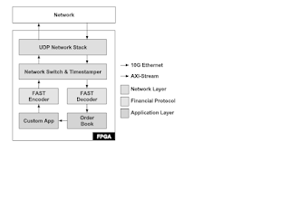
No comments:
Post a Comment